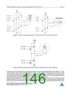
TMC4671 Datasheet • IC Version V1.00 | Document Revision V1.04 • 2018-Dec-11
142 / 157
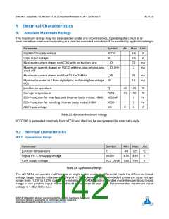
9 Electrical Characteristics
9.1 Absolute Maximum Ratings
The maximum ratings may not be exceeded under any circumstances. Operating the circuit at or
near more than one maximum rating at a time for extended periods shall be avoided by application design.
Parameter
Symbol
VCCIO
VI
Min Max Unit
Digital I/O supply voltage
3.6
3.6
70
3
V
Logic input voltage
V
Maximum current drawn on VCCIO with no load on pins
I_IO
mA
mA
Maximum current drawn on VCCIO with no load on pins and I_IO_0Hz
clock off
Maximum current drawn on V5 at fCLK = 25MHz
I_V5
25
10
mA
mA
Maximum current to / from digital pins and analog low voltage IIO
I/Os
Junction temperature
TJ
-40
-55
125
150
2
°C
°C
kV
kV
V
Storage temperature
TSTG
VESDAP
VESD1
VAI
ESD-Protection for interface pins (Human body model, HBM)
ESD-Protection for handling (Human body model, HBM)
ADC input voltage
2
0
5
Table 23: Absolute Maximum Ratings
VCCCORE is generated internally from VCCIO and shall not be overpowered by external supply.
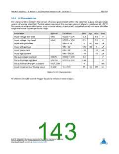
9.2 Electrical Characteristics
9.2.1 Operational Range
Parameter
Symbol
TJ
Min Max Unit
Junction temperature
Digital I/O 3.3V supply voltage
Core supply voltage
-40
125
°C
V
VIO3V
3.15 3.45
VCC_CORE 1.65 1.95
V
Table 24: Operational Range
The ∆Σ ADCs can operate in differential or single ended mode. In differential mode the differential input
voltage range must be in between -2.5V and +2.5V. However, it is recommended to use the input voltage
range from -1.25V to 1.25V, due to non-linearity of ∆Σ ADCs. In Single ended mode the operational input
range of the positive input channel should be between 0V and 2.5V. Recommended maximum input
voltage is 1.25V. ADCs have
©2018 TRINAMIC Motion Control GmbH & Co. KG, Hamburg, Germany
Terms of delivery and rights to technical change reserved.
Download newest version at www.trinamic.com

 TRINAMIC [ TRINAMIC MOTION CONTROL GMBH & CO. KG. ]