TMC4671 Datasheet • IC Version V1.00 | Document Revision V1.04 • 2018-Dec-11
138 / 157
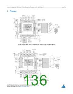
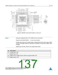
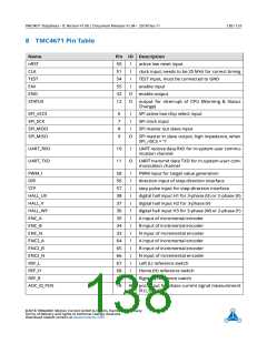
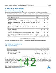
8 TMC4671 Pin Table
Name
nRST
CLK
Pin IO Description
50
51
54
55
32
12
I
I
active low reset input
clock input; needs to be 25 MHz for correct timing
TEST input, must be connected to GND
enable input
TEST
ENI
I
I
ENO
O
O
enable output
STATUS
output for interrupt of CPU (Warning & Status
Change)
SPI_nSCS
SPI_SCK
6
7
8
9
I
I
SPI active low chip select input
SPI clock input
SPI_MOSI
SPI_MISO
I
SPI master out slave input
O
SPI master in slave output, high impedance, when
SPI_nSCS = ’1’
UART_RXD
UART_TXD
10
11
I
UART receive data RxD for in-system-user commu-
nication channel
O
UART transmit data TXD for in-system-user com-
munication channel
PWM_I
DIR
58
56
57
38
37
36
35
34
33
64
65
66
67
68
69
16
I
I
I
I
I
I
I
I
I
I
I
I
I
I
I
PWM input for target value generation
direction input of step-direction interface
step pulse input for step-direction interface
digital hall input H1 for 3-phase (U) or 2-phase (X)
digital hall input H2 for 3-phase (V)
digital hall input H3 for 3-phase (W) or 2-phase (Y)
A input of incremental encoder
STP
HALL_UX
HALL_V
HALL_WY
ENC_A
ENC_B
ENC_N
ENC2_A
ENC2_B
ENC2_N
REF_L
B input of incremental encoder
N input of incremental encoder
A input of incremental encoder
B input of incremental encoder
N input of incremental encoder
Left (L) reference switch
REF_H
Home (H) reference switch
REF_R
Right (R) reference switch
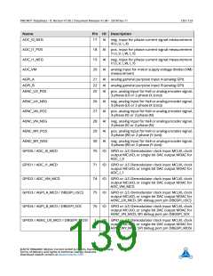
ADC_I0_POS
AI pos. input for phase current signal measurement
I0 (I_U, I_X)
©2018 TRINAMIC Motion Control GmbH & Co. KG, Hamburg, Germany
Terms of delivery and rights to technical change reserved.
Download newest version at www.trinamic.com

 TRINAMIC [ TRINAMIC MOTION CONTROL GMBH & CO. KG. ]