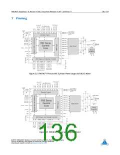
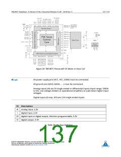
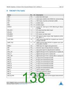
TMC4671 Datasheet • IC Version V1.00 | Document Revision V1.04 • 2018-Dec-11
140 / 157
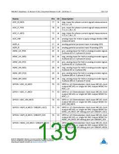
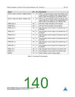
Name
Pin IO Description
GPIO6 / AENC_VN_MCD / DBGSPI_MISO
4
IO GPIO or ∆Σ-Demodulator clock input MCLKI, clock
output MCLKO, or single bit DAC output MDAC for
AGPI_A_MCD, SPI debug port pin DBGSPI_MISO
GPIO7 / AENC_WY_MCD / DBGSPI_TRG
5
IO GPIO or ∆Σ-Demodulator clock input MCLKI, clock
output MCLKO, or single bit DAC output MDAC for
AGPI_B_MCD, SPI debug port pin DBGSPI_TRG
PWM_IDLE_H
PWM_IDLE_L
PWM_UX1_H
59
60
39
I
I
idle level of high side gate control signals
idle level of low side gate control signals
O
high side gate control output U (3-phase) resp. X1
(2-phase)
PWM_UX1_L
PWM_VX2_H
PWM_VX2_L
PWM_WY1_H
PWM_WY1_L
40
41
42
46
47
O
O
O
O
O
low side gate control output U (3-phase) resp. X1
(2-phase)
high side gate control output V (3-phase) resp. X2
(2-phase)
low side gate control output V (3-phase) resp. X2
(2-phase)
high side gate control output W (3-phase) resp. Y1
(2-phase)
low side gate control output W (3-phase) resp. Y1
(2-phase)
PWM_Y2_H
PWM_Y2_L
BRAKE
48
49
31
O
O
O
high side gate control output Y2 (2-phase only)
low side gate control output Y2 (2-phase only)
brake chopper control output signal
Table 21: Functional Pin Description
©2018 TRINAMIC Motion Control GmbH & Co. KG, Hamburg, Germany
Terms of delivery and rights to technical change reserved.
Download newest version at www.trinamic.com

 TRINAMIC [ TRINAMIC MOTION CONTROL GMBH & CO. KG. ]