Features of the TMPM369FDFG/XBG (Under Development) and TMPM369FYFG/XBG (Under Development)
Qꢀ
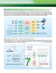
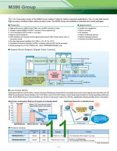
Controls various interfaces independently – Contributing to reduction of the CPU workload
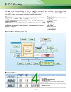
The TMPM369 has various external communication interfaces such as USB device, USB host, CAN, EtherMAC, SIO/UART,
I2C/SIO and SSP (SPI mode). Additionally, the TMPM369 contains 2 units of AD converter and a programmable motor driver
(PMD). All of them are designed to operate independently, significantly reducing the software workload. The TMPM369 provides
Flash ROM of up to 512 KB and SRAM of up to 128 KB to facilitate the use of the various communication interfaces.
M
M
USB 2.0
Device
PMD
2 ch
ARM
CortexTM-M3
USB 2.0
Host
12-bit ADC
12-bit ADC
SIO/UART
I2C/SIO
EtherMAC
CAN 2.0
NANO
FLASHTM
RAM
SSP
(SPImode)
Qꢀ
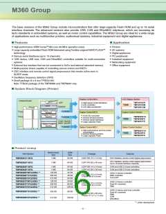
High-speed AD conversion – Using 2 units of AD converter
The TMPM369 contains 2 units of ADC. Their combined use provides high-speed AD conversion. While a single ADC offers a
minimum conversion time of 1.0 +s at 80 MHz, applying an analog signal to 2 units of ADC and using them in a time-interleaved
manner significantly reduces the conversion time required*.
*0.5 +s minimum (design target)
Timer
SW
Trigger
ADC
#1
CCD trigger
output
8 ch
Data 1 Data 3 Data 5
CCD data
output
ADC
#2
Data 2 Data 4 Data 6
A sample application using Barcode Read Control
0.5 +s 1.0 +s
–
–
7

 TOSHIBA [ TOSHIBA ]