TLP250H,TLP250HF
12. Switching Characteristics (Note)(Unless otherwise specified, Ta = -40 to 125 )
Test
Circuit
Characteristics
Symbol
Note
Test Condition
Min
100
Typ.
Max
500
Unit
ns
Propagation delay time
(L/H)
tpLH
(Note 1)
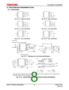
Fig.
IF = 0 → 10 mA, VCC = 30 V,
12.1.7 Rg = 20 Ω, Cg = 10 nF
Propagation delay time
(H/L)
tpHL
(Note 1)
IF = 10 → 0 mA, VCC = 30 V,
Rg = 20 Ω, Cg = 10 nF
100
50
50
500
50
Pulse width distortion
|tpHL-tpLH| (Note 1)
IF = 0 ←→ 10 mA, VCC = 30 V,
Rg = 20 Ω, Cg = 10 nF
Propagation delay skew
(device to device)
tpsk
tr
(Note 1),
(Note 4)
IF = 0 ←→ 10 mA, VCC = 30 V,
Rg = 20 Ω, Cg = 10 nF
-150
150
Rise time
(Note 1)
(Note 1)
(Note 2)
IF = 0 → 10 mA, VCC = 30 V,
Rg = 20 Ω, Cg = 10 nF
Fall time
tf
IF = 10 → 0 mA, VCC = 30 V,
Rg = 20 Ω, Cg = 10 nF
Common-mode transient
immunity at output high
CMH
Fig.
VCM = 1000 Vp-p, IF = 10 mA,
12.1.8 VCC = 30 V, Ta = 25 ,
±40
kV/µs
VO(min) = 26 V
Common-mode transient
immunity at output low
CML
(Note 3)
VCM = 1000 Vp-p, IF = 0 mA,
VCC = 30 V, Ta = 25 ,
VO(max) = 1 V
±40
Note: All typical values are at Ta = 25 .
Note 1: Input signal (f = 250 kHz, duty = 50 %, tr = tf = 5 ns or less).
CL is approximately 15 pF which includes probe and stray wiring capacitance.
Note 2: CMH is the maximum rate of rise of the common mode voltage that can be sustained with the output voltage
in the logic high state (VO > 26 V).
Note 3: CML is the maximum rate of fall of the common mode voltage that can be sustained with the output voltage in
the logic low state (VO < 1 V).
Note 4: The propagation delay skew, tpsk, is equal to the magnitude of the worst-case difference in tpHL and/or tpLH
that will be seen between units at the same given conditions (supply voltage, input current, temperature, etc).
©2015 Toshiba Corporation
2015-12-24
Rev.4.0
7
图片预览")
 TOSHIBA [ TOSHIBA ]