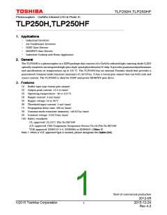
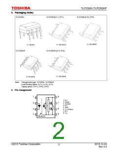
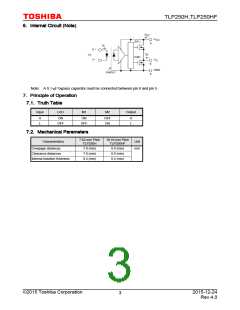
TLP250H,TLP250HF
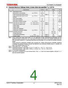
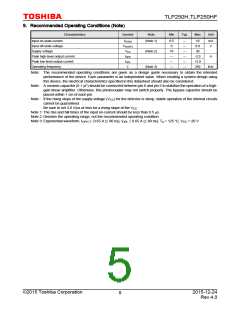
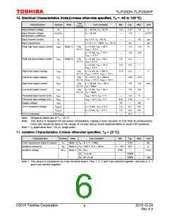
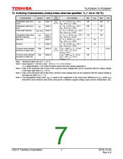
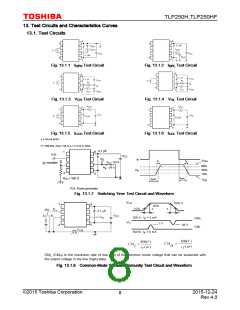
8. Absolute Maximum Ratings (Note) (Unless otherwise specified, Ta = 25 )
Characteristics
Symbol
Note
Rating
Unit
LED
Input forward current
IF
20
-0.54
1
mA
mA/
A
Input forward current derating
(Ta ≥ 110 )
(Ta ≥ 110 )
∆IF/∆Ta
IFPT
Peak transient input forward current
(Note 1)
Peak transient input forward current
derating
∆IFPT/∆Ta
-25
mA/
Input reverse voltage
VR
PD
6
40
V
mW
mW/
A
Input power dissipation
Input power dissipation derating
(Ta ≥ 110 )
∆PD/∆Ta
IOPH
IOPL
-1.0
Detector Peak high-level output current
Peak low-level output current
Output voltage
(Ta = -40 to 125 )
(Ta = -40 to 125 )
(Note 2)
(Note 2)
-2.5
+2.5
35
VO
V
Supply voltage
VCC
35
Output power dissipation
Output power dissipation derating
Common Operating temperature
Storage temperature
PO
260
mW
mW/
(Ta ≥ 110 )
∆PO/∆Ta
Topr
-2.0
-40 to 125
-55 to 150
260
Tstg
Lead soldering temperature
Isolation voltage
(10 s)
Tsol
(Note 3)
(Note 4)
AC, 60 s, R.H. ≤ 60 %
BVS
3750
Vrms
Note: Using continuously under heavy loads (e.g. the application of high temperature/current/voltage and the
significant change in temperature, etc.) may cause this product to decrease in the reliability significantly even
if the operating conditions (i.e. operating temperature/current/voltage, etc.) are within the absolute maximum
ratings.
Please design the appropriate reliability upon reviewing the Toshiba Semiconductor Reliability Handbook
("Handling Precautions"/"Derating Concept and Methods") and individual reliability data (i.e. reliability test
report and estimated failure rate, etc).
Note 1: Pulse width (PW) ≤ 1 µs, 300 pps
Note 2: Exponential waveform. Pulse width ≤ 0.2 µs, f ≤ 15 kHz, VCC = 20 V, Ta = -40 to 125
Exponential waveform. Pulse width ≤ 0.08 µs, f ≤ 25 kHz, VCC = 15V, Ta = -40 to 125
Note 3: ≥ 2 mm below seating plane.
Note 4: This device is considered as a two-terminal device: Pins 1, 2, 3 and 4 are shorted together, and pins 5, 6, 7
and 8 are shorted together.
©2015 Toshiba Corporation
2015-12-24
Rev.4.0
4
图片预览")
 TOSHIBA [ TOSHIBA ]