XC6101~XC6107, XC6111~XC6117 Series
■NOTES ON USE
1. Please use this IC within the stated maximum ratings. Operation beyond these limits may cause degrading or permanent
damage to the device.
2. When a resistor is connected between the VIN pin and the input, the VIN voltage drops while the IC is operating and a
malfunction may occur as a result of the IC’s through current. For the CMOS output products, the VIN voltage drops while
the IC is operating and malfunction may occur as a result of the IC’s output current. Please be careful with using the
XC6111~XC6117 series (without hysteresis).
3. In order to stabilize the IC’s operations, please ensure that the VIN pin’s input frequency’s rise and fall times are more than
1 µ sec/V.
4. Noise at the power supply may cause a malfunction of the watchdog operation or the circuit. In such case, please
strength the line between VIN and the GND pin and connect about 0.22µF of a capacitor between the VIN pin and the GND
pin.
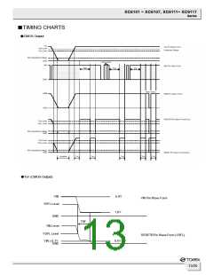
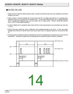
5. Protecting against a malfunction while the watchdog time out period, an ignoring time (no reaction time) occurs to the rise
and fall times. Referring to the figure below, the ignoring time (no reaction time) lasts for 900µsec at maximum.
VIN Pin Wave Form
TWD
TWD
GND
GND
WD Pin Wave Form
No reaction time
(MAX 900usec)
No reaction time
(MAX 900usec)
RESETB Pin Wave Form (VDFL)
TDR
TDR
GND
14/26

 TOREX [ Torex Semiconductor ]