XC6101~XC6107, XC6111~XC6117 Series
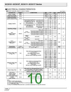
■ELECTRICAL CHARACTERISTICS
Ta = 25 OC
●XC6101~XC6107, XC6111~XC6117 Series
PARAMETER
Detect Voltage
Hysteresis Range
XC6101~XC6107 (*1)
Hysteresis Range
SYMBOL
CONDITIONS
MIN.
VDF(T)
× 0.98
VDF
TYP.
VDF(T)
VDF
MAX. UNITS CIRCUIT
VDFL
VDF(T)
V
V
V
1
1
1
VDFH
× 1.02
VDF
VHYS
× 0.02 × 0.05 × 0.08
VDF
VDF
VHYS
0
XC6111~XC6117 (*2)
× 0.001 x 0.01
XC61X1/XC61X2/XC61X3
XC61X4/XC61X5 (*3)
(The MRB & the WD Pin:
No connection)
VIN=VDF(T)×0.9V
VIN=VDF(T)×1.1V
VIN=6.0V
VIN=VDF(T)×0.9V
VIN=VDF(T)×1.1V
VIN=6.0V
-
-
-
-
-
5
10
12
4
11
16
18
10
14
16
6.0
-
Supply Current
ISS
VIN
µA
V
2
XC61X6/XC61X7 (*3)
(The MRB Pin:
8
No connection)
-
10
Operating Voltage
1.0
0.15
-
1
3
VIN=1.0V
0.5
VIN=2.0V (VDFL(T)> 2.0V)
VIN=3.0V (VDFL(T) >3.0V)
VIN=4.0V (VDFL(T) >4.0V)
2.0
3.0
3.5
2.5
3.5
4.0
-
-
-
N-ch.
VDS = 0.5V
VDFL
Output Current
(RESETB)
IRBOUT
mA
CMOS,
P-ch
VIN=6.0V
-
- 1.1
-0.8
4
3
VDS = 0.5V
N-ch
VIN=6.0V
4.4
4.9
-
VDS = 0.5V
VIN=1.0V
VIN=2.0V (VDFH(T)> 2.0V)
VIN=3.0V (VDFH(T)>3.0V)
-
-
-
-
- 0.08
- 0.50
- 0.75
- 0.95
- 0.02
- 0.30
- 0.55
- 0.75
VDFH
Output Current
(RESET)
IROUT
mA
P-ch.
4
1
VDS = 0.5V
VIN=4.0V (VDFH(T)>4.0V)
Temperature
△VDF /
ppm
O
O
-40 C < Topr < 85 C
-
+100
-
O
Characteristics
△Topr・VDF
/ C
2
13
25
60
120
240
960
2
13
25
60
120
240
960
3.13
25
50
100
200
400
1600
3.13
25
5
38
75
140
280
560
2240
5
38
75
140
280
560
2240
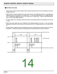
Time until VIN is increased from
1.0V to 2.0V
Release Delay Time
(VDF<1.8V)
TDR
and attains to the release
time level,
ms
5
and the Reset output pin inverts.
Time until VIN is increased from
1.0V to (VDFx1.1V)
50
Release Delay Time
(VDF>1.9V)
100
200
400
1600
TDR
TDF
and attains to the release
time level,
ms
5
5
and the Reset output pin inverts.
Time until VIN is decreased from 6.0V to
1.0V and attains to the detect voltage
level, and the Reset output pin detects
while the WD pin left opened.
Detect Delay Time
-
3
30
µs
VDFL/VDFH
CMOS Output
Leak Current
VDFL N-ch Open Drain
Output
VIN=6.0V, RESETB=6.0V (VDFL)
VIN=6.0V, RESET=0V (VDFH)
ILEAK
ILEAK
-
-
0.01
0.01
-
µA
µA
3
3
VIN=6.0V, RESETB=6.0V
0.10
Leak Current
NOTE:
*1: XC6101~XC6107 (with hysteresis)
*2: XC6111~XC6117 (without hysteresis)
*3: ‘X’ represents both ‘0’ and ‘1’. (ex. XC61X1⇒XC6101 and XC6111)
*4: VDF(T): Setting detect voltage
*5: If only “VDF” is indicated, it represents both VDFL (low when detected) and VDFH (high when detected).
10/26

 TOREX [ Torex Semiconductor ]