XC6101 ~ XC6107, XC6111~ XC6117
Series
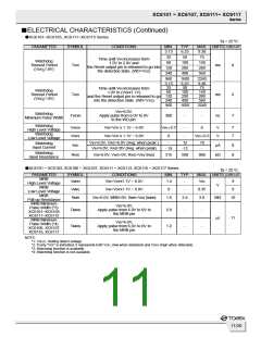
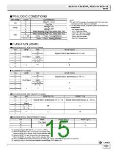
■PIN LOGIC CONDITIONS
PIN NAME
VIN
LOGIC
CONDITIONS
VIN>VDF+VHYS
NOTE:
H
L
*1: If only “VDF” is indicated, it represents both VDFL (low when
detected) and VDFH (high when detected).
*2: For the details of each parameter, please see the electrical
characteristics.
VIN<VDF
H
L
H
MRB>1.40V
MRB<0.35V
When keeping WD>VWDH more than TWD
When keeping WD<VWDL more than TWD
VWDL → VWDH, TWDIN>300nsec
VWDH →VWDH, TWDIN>300nsec
MRB
WD
VDF: Detect Voltage
VHYS: Hysteresis Range
VWDH: WD High Level Voltage
VWDL: WD Low Level Voltage
TWDIN: WD Pulse Width
L
L → H
H → L
TWD: WD Timeout Period
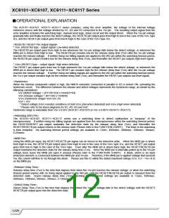
■FUNCTION CHART
●XC6101/XC61111, XC6102/6112 Series
VIN
H
H
H
H
H
H
L
MRB
WD
H
L
Open
L → H
H → L
RESETB (*2)
Repeat detect and release (H→L→H)
H or Open
H
L
L
*1
●XC6103/XC61113 Series
VIN
H
H
H
H
H
H
L
MRB
WD
H
L
Open
L → H
H → L
RESETB (*3)
Repeat detect and release (L→H→L)
H or Open
L
L
*1
H
●XC6104/XC61114, XC6105/XC6115 Series
VIN
H
H
H
H
H
H
L
WD
H
L
Open
L → H
H → L
RESETB (*2)
RESET (*3)
Repeat detect and release (H→L→H)
Repeat detect and release (L→H→L)
H
L
L
*1
H
●XC6106/XC61116, XC6107/XC6117 Series
VIN
H
MRB
H or Open
RESETB (*2)
RESET (*3)
L
H
H
L
L
L
H
*1: Including all logic of WD (WD=H, L, L→H, H→L, OPEN).
*2: When the RESETB is High, the circuit is in the release state.
When the RESETB is Low, the circuit is in the detection state.
*3: When the RESET is High, the circuit is in the release state.
When the RESET is Low, the circuit is in the detection state.
*4: VIN=L and MRB=H can not be combined for the rated input voltage of the MRB pin is Vss-0.3V to VIN+0.3V.
*5: The RESET/RESETB pin becomes indefinite operation while 0.35V<MRB<1.4V.
15/26

 TOREX [ Torex Semiconductor ]