XC6101~XC6107, XC6111~XC6117 Series
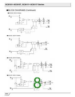
■OPERATIONAL EXPLANATION
The XC6101~XC6107, XC6111~XC6117 series compare, using the error amplifier, the voltage of the internal voltage
reference source with the voltage divided by R1, R2 and R3 connected to the VIN pin. The resulting output signal from the
error amplifier activates the watchdog logic, manual reset logic, delay circuit and the output driver. When the VIN pin voltage
gradually falls and finally reaches the detect voltage, the RESETB pin output goes from high to low in the case of the VDFL type
ICs, and the RESET pin output goes from low to high in the case of the VDFH type ICs.
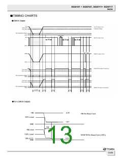
<RESETB / RESET Pin Output Signal>
* VDFL (RESETB) type - output signal: Low when detected.
The RESETB pin output goes from high to low whenever the VIN pin voltage falls below the detect voltage, or whenever the
MRB pin is driven from high to low. The RESETB pin remains low for the release delay time (TDR) after the VIN pin voltage
reaches the release voltage. If neither rising nor falling signals are applied to the WD pin within the watchdog timeout period,
the RESETB pin output remains low for the release delay time (TDR), and thereafter the RESET pin outputs high level signal.
* VDFH (RESET) type – output signal: High when detected.
The RESET pin output goes from low to high whenever the VIN pin voltage falls below the detect voltage, or whenever the
MRB pin is driven from high to low. The RESET pin remains high for the release delay time (TDR) after the VIN pin voltage
reaches the release voltage. If neither rising nor falling signals are applied to the WD pin within the watchdog timeout period,
the VOUT pin output remains high for the release delay time (TDR), and thereafter the RESET pin outputs low level signal.
<Hysteresis>
When the internal comparator output is high, the NMOS transistor connected in parallel to R3 is turned ON, activating the
hysteresis circuit. The difference between the release and detect voltages represents the hysteresis range, as shown by the
following calculations:
VDF (detect voltage) = (R1+R2+R3) x Vref(R2+R3)
VDR (release voltage) = (R1+R2) x Vref(R2)
VHYS (hysteresis range)=VDR-VDF (V)
VDR > VDF
* Detect voltage (VDF) includes conditions of both VDFL (low when detected) and VDFH (high when detected).
* Please refer to the block diagrams for R1, R2, R3 and Vref.
Hysteresis range is selectable from VDF x 0.05V (XC6101~XC6107) or VDF x 0.001V (XC6111~XC6117).
<Watchdog (WD) Pin>
The XC6101~XC6107, XC6111~XC6117 series use a watchdog timer to detect malfunction or “runaway” of the
microprocessor. If neither rising nor falling signals are applied from the microprocessor within the watchdog timeout period,
the RESETB/RESET pin output maintains the detection state for the release delay time (TDR), and thereafter the
RESET/RESETB pin output returns to the release state (Please refer to the FUNCTION CHART). The timer in the watchdog
is then restarted. Six watchdog timeout period settings are available in 1.6sec, 400msec, 200msec, 100msec, 50msec,
6.25msec.
<MRB Pin>
Using the MRB pin input, the RESET/RESETB pin signal can be forced to the detection state. When the MRB pin is driven
from high to low, the RESETB pin output goes from high to low in the case of the VDFL type ICs, and the RESET pin output
goes from low to high in the case of the VDFH type. Even after the MRB pin is driven back high, the RESET/RESETB pin
output maintains the detection state for the release delay time (TDR). Since the MRB pin is internally pulled up to the VIN pin
voltage level, leave the MRB pin open if unused (Please refer to the FUNCTION CHART). A diode, which is an input
protection element, is connected between the MRB pin and VIN pin. Therefore, if the MRB pin is applied voltage that exceeds
VIN, the current will flow to VIN through the diode. Please use this IC within the stated maximum ratings (VSS -0.3 ~ VIN +0.3)
on the MRB pin.
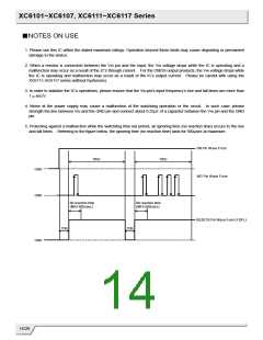
<Release Delay Time>
Release delay time (TDR) is the time that elapses from when the VIN pin reaches the release voltage, or when the watchdog
timeout period expires with no rising signal applied to the WD pin, until the RESET/RESETB pin output is released from the
detection state. Seven release delay time (TDR) watchdog timeout period settings are available in 1.6sec, 400msec,
200msec, 100msec, 50msec, 25msec, 3.13msec.
<Detect Delay Time>
Detect Delay Time (TDF) is the time that elapses from when the VIN pin voltage falls to the detect voltage until the RESET/
RESETB pin output goes into the detection state.
12/26

 TOREX [ Torex Semiconductor ]