ꢠꢆ ꢁ ꢡꢡꢢ
www.ti.com
SBOS344 − SEPTEMBER 2005
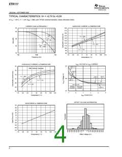
MINIMUM OUTPUT CURRENT
MAXIMUM OUTPUT CURRENT
The quiescent current of the XTR117 (typically 130µA)
The XTR117 provides accurate, linear output up to
25mA. Internal circuitry limits the output current to
approximately 32mA to protect the transmitter and loop
power/measurement circuitry.
is the lower limit of its output current. Zero input current
(I = 0) will produce an I equal to the quiescent current.
IN
O
Output current will not begin to increase until
> I /100. Current drawn from V will be added to
I
IN
Q
REG
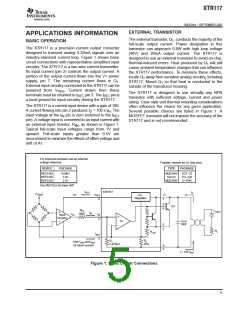
It is possible to extend the output current range of the
XTR117 by connecting an external resistor from pin 3
to pin 5, to change the current limit value. Since all
output current must flow through internal resistors, it is
possible to cause internal damage with excessive
current. Output currents greater than 45mA may cause
permanent damage.
this minimum output current. Up to 3.8mA is available
to power external circuitry while still allowing the output
current to go below 4mA.
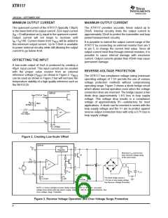
OFFSETTING THE INPUT
A low-scale output of 4mA is produced by creating a
40µA input current. This input current can be created
with the proper value resistor from an external
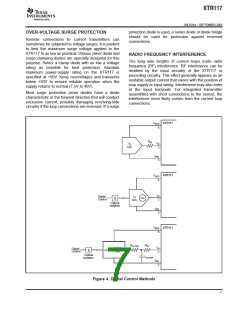
REVERSE-VOLTAGE PROTECTION
reference voltage (V
) as shown in Figure 2. V
REF
REG
The XTR117 low compliance voltage rating (minimum
operating voltage) of 7.5V permits the use of various
voltage protection methods without compromising
operating range. Figure 3 shows a diode bridge circuit
which allows normal operation even when the voltage
connection lines are reversed. The bridge causes a two
diode drop (approximately 1.4V) loss in loop supply
voltage. This voltage drop results in a compliance
voltage of approximately 9V—satisfactory for most
applications. A diode can be inserted in series with the
loop supply voltage and the V+ pin to protect against
reverse output connection lines with only a 0.7V loss in
loop supply voltage.
can be used as shown in Figure 2 but will not have the
temperature stability of a high quality reference such as
the REF3125.
XTR117
VREG
8
VREF (2.5V) or
...................
R
Ω
62.5kIN
40 A
µ
IIN
2
A1
0 to 160 A
µ
IRET
3
R1
2.475k
Ω
Figure 2. Creating Low-Scale Offset
XTR117
VREG
V+
7
+5V
Regulator
8
Maximum VPS must be less
than minimum voltage rating
of the zener diode.
B
6
Q1
RIN
IIN
2
A1
(1)
µ
0.01
F
D1
IN4148
E
5
VIN
RLIM
VLOOP
RL
IRET
3
IO = 100 VIN
RIN
R1
2.475k
R2
25
The diode bridge causes a
1.4V loss in loop supply voltage.
See Reverse−Voltage Protection.
Ω
Ω
4
NOTE: (1) Some examples of zener diodes include: P6KE51 or 1N4755A. Use lower
voltage zener diodes with loop power−supply voltages < 30V for increased protection. See
Over−voltage Surge Protection.
Figure 3. Reverse Voltage Operation and Over-Voltage Surge Protection
6

 TI [ TEXAS INSTRUMENTS ]