ꢠꢆ ꢁ ꢡꢡꢢ
www.ti.com
SBOS344 − SEPTEMBER 2005
(1)
ELECTROSTATIC DISCHARGE SENSITIVITY
ABSOLUTE MAXIMUM RATINGS
Power Supply, V+ (referenced to I pin) . . . . . . . . . . . . . . . . +50V
O
This integrated circuit can be damaged by ESD. Texas
Instruments recommends that all integrated circuits be
handledwith appropriate precautions. Failure to observe
Input Voltage, (referenced to I
pin) . . . . . . . . . . . . . . . 0V to V+
RET
Output Current Limit . . . . . . . . . . . . . . . . . . . . . . . . . . . . Continuous
, Short-Circuit . . . . . . . . . . . . . . . . . . . . . . . . . . . . Continuous
V
REG
proper handling and installation procedures can cause damage.
Operating Temperature Range . . . . . . . . . . . . . . . −55°C to +125°C
Storage Temperature Range . . . . . . . . . . . . . . . . . −55°C to +125°C
Junction Temperature . . . . . . . . . . . . . . . . . . . . . . . . . . . . . . . +165°C
ESD Rating (Human Body Model) . . . . . . . . . . . . . . . . . . . . . . . 2000V
(Charged Device Model) . . . . . . . . . . . . . . . . . 1000V
ESD damage can range from subtle performance degradation to
complete device failure. Precision integrated circuits may be more
susceptible to damage because very small parametric changes could
cause the device not to meet its published specifications.
(1)
Stresses above these ratings may cause permanent damage.
Exposure to absolute maximum conditions for extended periods
may degrade device reliability. These are stress ratings only, and
functional operation of the device at these or any other conditions
beyond those specified is not implied.
(1)
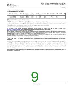
PACKAGE/ORDERING INFORMATION
PACKAGE
DESIGNATOR
PACKAGE
MARKING
TRANSPORT MEDIA,
QUANTITY
PRODUCT
PACKAGE-LEAD
ORDERING NUMBER
XTR117AIDGKT
XTR117AIDGKR
XTR117AIDRBT
XTR117AIDRBR
Tape and Reel, 250
Tape and Reel, 2500
Tape and Reel, 250
Tape and Reel, 3000
XTR117
MSOP-8
DGK
DRB
BOZ
BOY
(2)
XTR117
DFN-8
(1)
(2)
For the most current package and ordering information, see the Package Option Addendum located at the end of this data sheet.
Available Q1 2006.
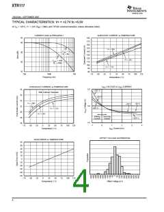
PIN ASSIGNMENTS
Top View
XTR117
XTR117
NC(1)
IIN
VREG
NC(1)
IIN
1
2
3
4
8
7
6
5
VREG
1
2
3
4
8
7
6
5
Exposed
Thermal
Die Pad
on
V+
V+
IRET
IO
B (Base)
E (Emitter)
IRET
IO
B (Base)
E (Emitter)
Underside(2)
MSOP−8
DFN−8(3)
NOTES: (1) NC = No connection. Leave unconnected on PCB.
−
(2) Connect thermal die pad to V .
(3) Available Q1 2006.
2

 TI [ TEXAS INSTRUMENTS ]