ꢠ ꢆꢁꢡꢡ ꢢ
www.ti.com
SBOS344 − SEPTEMBER 2005
EXTERNAL TRANSISTOR
APPLICATIONS INFORMATION
BASIC OPERATION
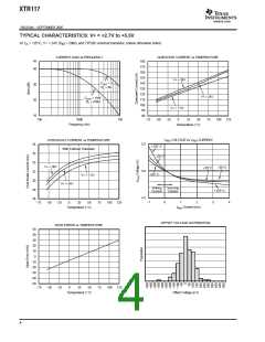
The external transistor, Q , conducts the majority of the
1
full-scale output current. Power dissipation in this
transistor can approach 0.8W with high loop voltage
(40V) and 20mA output current. The XTR117 is
designed to use an external transistor to avoid on-chip,
thermal-induced errors. Heat produced by Q will still
cause ambient temperature changes that can influence
the XTR117 performance. To minimize these effects,
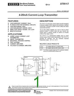
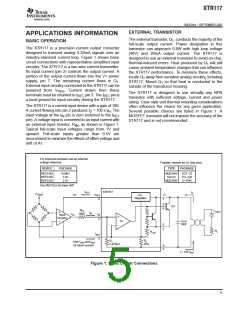
The XTR117 is a precision current output converter
designed to transmit analog 4-20mA signals over an
industry-standard current loop. Figure 1 shows basic
circuit connections with representative simplified input
circuitry. The XTR117 is a two-wire current transmitter.
Its input current (pin 2) controls the output current. A
portion of the output current flows into the V+ power
1
locate Q away from sensitive analog circuitry, including
1
supply, pin 7. The remaining current flows in Q .
1
XTR117. Mount Q so that heat is conducted to the
1
External input circuitry connected to the XTR117 can be
outside of the transducer housing.
powered from V
. Current drawn from these
REG
The XTR117 is designed to use virtually any NPN
transistor with sufficient voltage, current and power
rating. Case style and thermal mounting considerations
often influence the choice for any given application.
Several possible choices are listed in Figure 1. A
MOSFET transistor will not improve the accuracy of the
XTR117 and is not recommended.
terminals must be returned to I , pin 3. The I
pin is
RET
RET
a local ground for input circuitry driving the XTR117.
The XTR117 is a current-input device with a gain of 100.
A current flowing into pin 2 produces I = 100 x I . The
O
IN
input voltage at the I pin is zero (referred to the I
IN
RET
pin). A voltage input is converted to an input current with
an external input resistor, R , as shown in Figure 1.
IN
Typical full-scale input voltages range from 1V and
upward. Full-scale inputs greater than 0.5V are
recommend to minimize the effects of offset voltage and
drift of A1.
For improved precision use an external
voltage reference.
Possible choices for Q1 (see text):
DEVICE
VOLTAGE
TYPE
PACKAGE
REF3140
REF3130
REF3125
4.096V
3.0V
2.5V
MJE3440
TIP41C
MJD3340
SOT−32
TO−220
D−PAK
Use REF32xx for lower drift.
IREG
XTR117
IO
(VREF
)
VREG
8
5V
V+
+5V
Regulator
7
B
6
Q1
RIN
VLOOP
IIN
Ω
20k
VIN
IIN
2
Input
Circuitry
COUT
10nF
A1
E
5
RL
RLIM
IRET
3
R1
2.475k
R2
25
from IREG and IREF
All return current
Ω
Ω
IO
4
I = 100 (IIN
)
Figure 1. Basic Circuit Connections
5

 TI [ TEXAS INSTRUMENTS ]