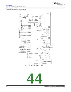
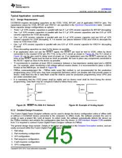
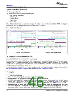
UCD90320
www.ti.com.cn
ZHCSFI3B –AUGUST 2016–REVISED MAY 2019
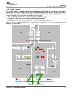
11.2 Layout Example
The UCD90320 device is available in a 169-pin BGA package. If the design calls for the device to be mounted on
the top layer, decoupling capacitors can be placed on the bottom layer to allow room for top-layer trace routing.
The layout example below describes this strategy. Figure 43 shows bottom-layer component placement from top-
view. In addition to Figure 43, consider these important suggestions.
1. Use a uniform ground plane to connect DVSS, AVSS, and VREFA– pins.
2. Connect all four BPCAP pins to a common internal-layer copper area.
3. AVSS and VREFA– pins can be connected to a common internal-layer copper area.
Figure 43 shows a typical application with the UCD90320 device mounted on the top layer and the components
placed on the bottom layer.
V33D
R
C
C
C
C
C
C
GND
GND
MO
N1
2
N1
1
A1
MO
JT
AG
_T
MO
N1
3
LG LG
GP MR MR
IO2 GN GN
V33A
VREFA+
DV
SS
PO PO
MR
GN
MR
PM
3
GN
BU
4
1
14 18
DV GP
PM
CK
C
C
C
C
SS IO8
BU
C
C
3
13
S
PM
S
_C
MR
GN
7
B
NT
AL
GP
IO1
Un
3
use
_C
LK
MO MO
N4 N3
DV
SS
MO MO
N1 N1
RE GP
RL
ER
V33D
SE IO1
T
T#
5
d-
NC
GP GP
IO1 IO1
8
7
DV
SS
DV
DV
SS
6
9
DV
DV
SS
EN EN EN EN
Un
SS
use
SS
MR
BPCAP
GN
MR
10
d-
13 10
6
4
GP
IO2
DV
EN EN EN EN GP
Un
C
C
GN
SS
3 IO9
use GP
14
9
5
EN EN EN
LG LG
PO PO
10 11
MR
GN
MR
2
0
Un
GN
use
21
d- IO1
GP
IO1
12
8
1
MR
23
DV
SS
2
GP GP
UCD90320
IO2 IO4
GN
8
d-
1
DV
SS
BPCAP
C
C
C
C
GND
GND
V33D
V33A
BPCAP
VREFA+
BPCAP to be connected to decoupling capacitors through an internal-layer copper area
Figure 43. Layout Example
版权 © 2016–2019, Texas Instruments Incorporated
47

 TI [ TEXAS INSTRUMENTS ]