UCD8220, UCD8620
www.ti.com
SLUS652B–MARCH 2005–REVISED SEPTEMBER 2005
ELECTRICAL CHARACTERISTICS (continued)
VDD = 12 V, 4.7-µF capacitor from VDD to AGND, 1 µF from PVDD to PGND, 0.22-µF capacitor from 3V3 to AGND,
TA = TJ = -40°C to 105°C, (unless otherwise noted).
PARAMETER
ISET resistor range
TEST CONDITIONS
MIN
6.19
4.99
TYP
MAX UNIT
Current mode control; RISET connected to AGND
Voltage mode control; RISET connected to 3V3
499
kΩ
ISET resistor range
402
Voltage mode control with Feed-Forward; RISET connected to
VIN
ISET current range
3.7
300
0.6
µA
PWM
PWM offset at CTRL input
CTRL buffer gain(1)
3V3 = 3.3 V +/-2%
0.45
0.51
0.5
V
Gain from CTRL to PWM comparator input
V/V
CURRENT LIMIT (ILIM)
ILIM internal current limit threshold
ILIM = OPEN
0.466
0.975
0.700
0.21
2.64
-
0.5
1.025
0.725
0.23
-
0.536
1.075
0.750
0.25
-
V
V
ILIM maximum current limit threshold ILIM = 3.3 V
ILIM current limit threshold ILIM = 0.75 V
ILIM minimum current limit threshold ILIM = 0.25 V
V
CLF output high level
CS > ILIM , ILOAD = -7 mA
V
CLF output low level
CS ≤ ILIM, ILOAD = 7 mA
-
0.66
25
Propagation delay from CLK to CLF
CURRENT SENSE COMPARATOR
Bias voltage
CLK rising to CLF falling after a current limit event
-
15
ns
Includes CS comp offset
5
-
25
–1
25
25
50
-
mV
Input bias current
µA
Propagation delay from CS to OUTx ILIM = 0.5 V, measured on OUTx, CS = threshold + 60 mV
Propagation delay from CS to CLF ILIM = 0.5 V, measured on CLF, CS = threshold + 60 mV
CURRENT SENSE DISCHARGE TRANSISTOR
-
40
50
ns
-
Discharge resistance
CLK = low, resistance from CS to AGND
10
35
75
Ω
OUTPUT DRIVERS
(2)
Source current
VDD = 12 V, CLK = high, OUTx = 5 V
VDD = 12 V, CLK = low, OUTx = 5 V
VDD = 4.75 V, CLK = high, OUTx = 0
VDD = 4.75 V, CLK = low, OUTx = 4.75 V
CLOAD = 2.2 nF, VDD = 12 V
-
-
-
-
-
-
-
-
4
4
-
-
(2)
Sink current
A
Source current(2)
2
-
(2)
Sink current
3
-
Rise time, tR
10
10
0.8
25
25
20
15
1.2
35
35
ns
V
Fall time, tF
CLOAD = 2.2 nF, VDD = 12 V
Output with VDD < UVLO
VDD = 1.0 V, ISINK = 10 mA
CLOAD = open, VDD = 12 V, CLK rising, tD1
CLOAD = open, VDD = 12 V, CLK falling, tD2
Propagation delay from CLK to OUTx
ns
(2) Ensured by design. Not 100% tested in production.
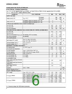
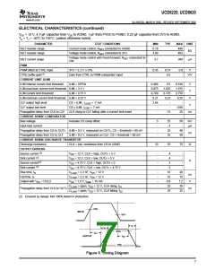
VIT+
INPUT
VIT−
t
F
t
F
90%
t
D1
t
OUTPUT
D2
10%
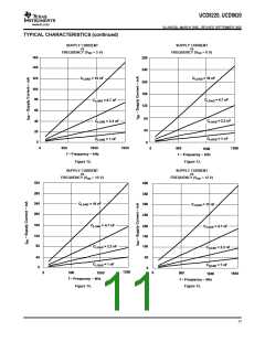
Figure 5. Timing Diagram
7

 TI [ TEXAS INSTRUMENTS ]