UCD8220, UCD8620
www.ti.com
SLUS652B–MARCH 2005–REVISED SEPTEMBER 2005
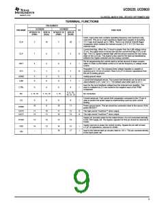
TERMINAL FUNCTIONS
PIN NUMBER
UCD8220
HTSSOP-16 QFN-16
UCD8620
PIN NAME
I/O
FUNCTION
HTSSOP-16
(PWP)
QFN-20
(RGW)
(PWP)
(RSA)
Clock. Input pulse train contains operating frequency and maximum duty
cycle limit. This pin is a high impedance digital input capable of accepting
3.3-V logic level signals up to 2 MHz. There is an internal Schmitt trigger
comparator which isolates the internal circuitry CLK 2 16 2 20 I from any
external noise.
CLK
2
16
2
7
20
5
I
Current limit flag. When the CS level is greater than the ILIM voltage minus
25 mV, the output driver is forced low and the current limit flag (CLF) is set
high. The CLF signal is latched high until the device receives the next rising
edge on the CLK pin. This signal is also used for the start-up handshaking
between the Digital controller and the analog controller
CLF
7
5
O
Pin for programming the current used to set the amount of slope compen-
sation in Peak-Current Mode control or to set the frequency in voltage mode
control.
ISET
3V3
4
3
2
1
4
3
2
1
I
Regulated 3.3-V rail. The onboard linear voltage regulator is capable of
sourcing up to 10 mA of current. Place 0.22 µF of ceramic capacitance from
this pin to analog ground.
O
AGND
ILIM
5
8
3
6
5
8
3
7
-
I
Analog ground return
Current limit threshold set pin. The current limit threshold can be set to any
value between 0.25 V and 1.0 V. The default value while open is 0.5 V.
Input for the error feedback voltage from the external error amplifier. This
input is multiplied by 0.5 and routed to the negative input of the PWM
comparator
CTRL
NC
6
4
6
4
I
6, 8, 10,
16, 18, 19
1, 15, 16
7, 14, 15
1, 15
-
No connection.
Current sense pin. Fast current limit comparator connected to the CS pin is
used to protect the power stage by implementing cycle-by-cycle current
limiting.
CS
9
8
9
9
9
I
10
10
11
-
Power ground return. This pin should be connected close to the source of the
power MOSFET.
PGND
OUT2
OUT1
11
12
10
11
11
12
12
13
O
O
The high-current TrueDrive™ driver output.
The high-current TrueDrive™ driver output.
Supply pin provides power for the output drivers. It is not connected internally
to the VDD supply rail. The bypass capacitor for this pin should be returned to
PGND.
PVDD
13
12
13
14
Supply input pin to power the control circuitry. Bypass the pin with at least
4.7 µF of capacitance, returned to AGND.
VDD
VIN
14
-
13
-
14
16
15
17
I
I
Input to the internal start-up circuitry rated to 110 V. This pin connects directly
to the input power rail.
9

 TI [ TEXAS INSTRUMENTS ]