UCD8220, UCD8620
www.ti.com
SLUS652B–MARCH 2005–REVISED SEPTEMBER 2005
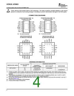
PACKAGING INFORMATION
POWER RATING TA
= 70°C, TJ = 125°C
(mW)
RATING FACTOR
ABOVE 70°C
(mW/°C)
PACKAGE
SUFFIX
θJC(°C/W)
θJA(°C/W)
PowerPad™
MSSOP-16
PWP
2.07
37.47(1)
1470
27
QFN-16
QFN-20
RSA
-
-
-
-
-
-
-
-
RGW
(1) PowerPad™ soldered to the PWB with TI recommended PWB as defined in TI's Application Report ( TI Literature Number SLMA002)
with OLFM.
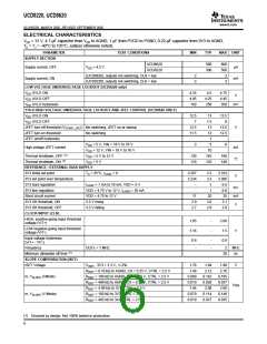
ABSOLUTE MAXIMUM RATINGS(1)(2)
SYMBOL
PARAMETER
UCD8x20
110
UNIT
VI
VDD
Input Line Voltage
Supply Voltage
UCD8620 only
V
16
Quiescent
20
IDD
Supply Current
mA
V
Switching, TA = 25°C, TJ = 125°C, VDD = 12 V
200
VO
Output Gate Drive Voltage
Output Gate Drive Current
OUT
-1 to PVDD
4.0
IO(sink)
IO(source)
OUT
A
-4.0
Analog Input
Digital I/O’s
ISET, CS, CTRL, ILIM
CLK, CLF
-0.3 to 3.6
-0.3 to 3.6
2.67
V
TA = 25°C (PWP-16 package)
TA = 25°C (QFN-16 package)
TA = 25°C (QFN-20 package)
UCD8220
W
Power Dissipation
-
-
-55 to 150
-55 to 130
-65 to 150
2000
Junction Operating
Temperature
TJ
UCD8620
°C
Tstg
Storage Temperature
ESD Rating(3)
HBM
CDM
Human body model
V
Change device model
500
Lead Temperature (Soldering, 10 sec)
300
°C
(1) Stresses beyond those listed under “absolute maximum ratings” may cause permanent damage to the device. These are stress ratings
only, and functional operation of the device at these or any other conditions beyond those indicated under “recommended operating
conditions” is not implied. Exposure to absolute-maximum-rated conditions for extended periods may affect device reliability.
(2) All voltages are with respect to GND. Currents are positive into, negative out of the specified terminal.
(3) Tested to JEDEC standard EIA/JESD22 - A114-B.
5

 TI [ TEXAS INSTRUMENTS ]