ꢀ ꢁꢁꢂ ꢃ ꢄ ꢅ ꢆ ꢀ ꢁꢁ ꢂ ꢃꢄ ꢃ ꢆ ꢀꢁ ꢁꢇ ꢃ ꢄ ꢅ ꢆ ꢀꢁ ꢁꢇ ꢃ ꢄ ꢃ
ꢈ ꢉꢁꢊ ꢋꢌ ꢍꢋꢎ ꢏꢐ ꢑꢒꢁ ꢓꢋ ꢐ ꢍ ꢐꢏ ꢐꢏ ꢔꢀ ꢕꢒꢓꢋ ꢐ
ꢖ
SLUS395J - FEBRUARY 2000 - REVISED MARCH 2009
APPLICATION INFORMATION
start up
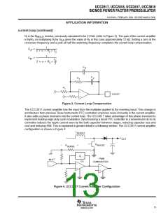
The UCC3818 version of the device is intended to have VCC connected to a 12-V supply voltage. The UCC3817
has an internal shunt regulator enabling the device to be powered from bootstrap circuitry as shown in the typical
application circuit of Figure 1. The current drawn by the UCC3817 during undervoltage lockout, or start-up
current, is typically 150 µA. Once VCC is above the UVLO threshold, the device is enabled and draws 4 mA
typically. A resistor connected between the rectified ac line voltage and the VCC pin provides current to the shunt
regulator during power up. Once the circuit is operational, the bootstrap winding of the inductor provides the
VCC voltage. Sizing of the start-up resistor is determined by the start-up time requirement of the system design.
DV
Dt
I
+ C
C
(
)
V
0.9
RMS
I
R +
C
Where I is the charge current, C is the total capacitance at the VCC pin, ∆V is the UVLO threshold and ∆t is
C
the allowed start-up time.
Assuming a 1 second allowed start-up time, a 16-V UVLO threshold, and a total VCC capacitance of 100 µF,
a resistor value of 51 kΩ is required at a low line input voltage of 85 V
small as to be ignored in sizing the start-up resistor.
. The IC start-up current is sufficiently
RMS
capacitor ripple reduction
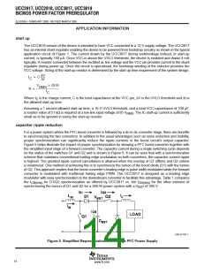
For a power system where the PFC boost converter is followed by a dc-to-dc converter stage, there are benefits
to synchronizing the two converters. In addition to the usual advantages such as noise reduction and stability,
proper synchronization can significantly reduce the ripple currents in the boost circuit’s output capacitor.
Figure 5 helps illustrate the impact of proper synchronization by showing a PFC boost converter together with
the simplified input stage of a forward converter. The capacitor current during a single switching cycle depends
on the status of the switches Q1 and Q2 and is shown in Figure 6. It can be seen that with a synchronization
scheme that maintains conventional trailing-edge modulation on both converters, the capacitor current ripple
is highest. The greatest ripple current cancellation is attained when the overlap of Q1 offtime and Q2 ontime
is maximized. One method of achieving this is to synchronize the turnon of the boost diode (D1) with the turnon
of Q2. This approach implies that the boost converter’s leading edge is pulse width modulated while the forward
converter is modulated with traditional trailing edge PWM. The UCC3817 is designed as a leading edge
modulator with easy synchronization to the downstream converter to facilitate this advantage. Table 1 compares
the I
for D1/Q2 synchronization as offered by UCC3817 vs. the I
for the other extreme of
of 385 V.
CB(rms)
CB(rms)
synchronizing the turnon of Q1 and Q2 for a 200-W power system with a V
BST
UDG-97130-1
Figure 5. Simplified Representation of a 2-Stage PFC Power Supply
14
www.ti.com

 TI [ TEXAS INSTRUMENTS ]