UCC28610
www.ti.com ......................................................................................................................................... SLUS888C–JANUARY 2009–REVISED SEPTEMBER 2009
DEVICE INFORMATION
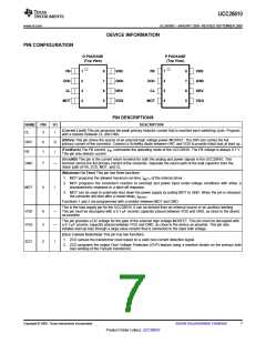
PIN CONFIGURATION
D PACKAGE
(Top View)
P PACKAGE
(Top View)
FB
ZCD
CL
1
8
7
6
5
VDD
GND
DRV
VGG
FB
ZCD
CL
1
8
7
6
5
VDD
GND
DRV
VGG
2
3
4
2
3
4
MOT
MOT
PIN DESCRIPTIONS
NAME PIN
I/O
DESCRIPTION
(Current Limit) This pin programs the peak primary inductor current that is reached each switching cycle. Program
with a resistor between CL and GND.
CL
3
6
1
I
(DRiVe) This pin drives the source of an external high voltage power MOSFET. The DRV pin carries the full
primary current of the converter. Connect a Schottky diode between DRV and VDD to provide initial bias at start up.
DRV
FB
O
I
(FeedBack) The FB current, IFB, commands the operating mode of the UCC28610. The FB voltage is always 0.7 V.
This pin only detects current.
(GrouND) This pin is the current return terminal for both the analog and power signals in the UCC28610. This
terminal carries the full primary current of the converter. Separate the return path of the bulk capacitor from the
return path of FB, ZCD, MOT, and CL.
GND
7
—
(Maximum On Time) This pin has three functions:
1. MOT programs the allowed maximum on-time, tMOT, of the internal driver.
2. MOT programs the converter’s reaction to overload and power input under-voltage conditions with either a
shutdown/retry response or a latch-off response.
MOT
4
I
3. MOT can be used to externally shut down the power supply by pulling MOT to GND. When the pin is released,
the converter will start after a restart delay, tRETRY
.
Functions 1 and 2 are programmed with a resistor between MOT and GND.
This is the bias supply pin for the UCC28610. It can be derived from an external source or an auxiliary winding.
This pin must be decoupled with a 0.1-µF ceramic capacitor placed between VDD and GND, as close to the device
as possible.
VDD
VGG
8
5
—
—
This pin provides a DC voltage for the gate of the external high voltage MOSFET. This pin must be decoupled with
a 0.1-µF ceramic capacitor placed between VGG and GND, as close to the device as possible. This pin also
initiates start-up bias through a large value resistor that is connected to the input bulk voltage.
(Zero Current Detection) This pin has two functions:
1. ZCD senses the transformer reset based on a valid zero current detection signal.
ZCD
2
I
2. ZCD programs the output Over Voltage Protection (OVP) feature using a resistive divider on the primary side
bias winding of the Flyback transformer.
Copyright © 2009, Texas Instruments Incorporated
Submit Documentation Feedback
7
Product Folder Link(s): UCC28610

 TI [ TEXAS INSTRUMENTS ]