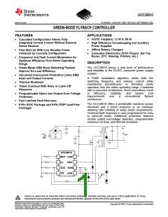
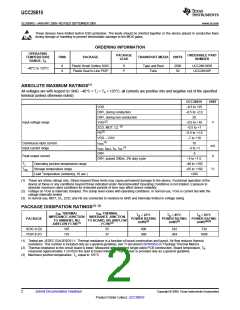
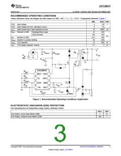
UCC28610
www.ti.com ......................................................................................................................................... SLUS888C–JANUARY 2009–REVISED SEPTEMBER 2009
ELECTRICAL CHARACTERISTICS (continued)
Unless otherwise stated: VDD = 12 V, VGG=12 V, ZCD = 1 V, FB = 0 V, GND = 0 V, a 0.1-µF capacitor between VDD and
GND, a 0.1-µF capacitor between VGG and GND, RCL = 33.2 kΩ, RMOT = 380 kΩ, –40°C < TA < +125°C, TJ = TA
PARAMETER
TEST CONDITIONS
MIN
TYP
MAX UNITS
VFB
Voltage of FB pin
IFB = 10 µA
0.34
0.7
0.84
V
ZERO CROSSING DETECTION
ZCD high to low generates switching period
(tS has expired)
ZCD(TH)
ZCD zero crossing threshold
5
-200
0.1
20
-160
0.15
50
-100
0.2
mV
mV
V
ZCD(CLAMP)
ZCD(START)
ZCD low clamp voltage
IZCD = –10 µA
ZCD voltage threshold to enable
the internal start timer
Driver switching periods generated at start
timer rate
Delay from zero crossing to Driver
turn-on
tDLY(ZCD)
150-Ω pull-up to 12-V on DRV
150
ns
Wait time for zero crossing
detection
Driver turn-on edge generated following tS
with previous zero crossing detected
tWAIT(ZCD)
2
2.4
2.8
µs
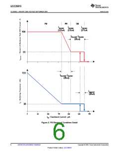
tST
Starter time-out period
ZCD = 0 V
150
240
300
DRIVER
RDS(on)(DRV)
IDRV(OFF)
RDS(on)(HSDRV)
IDRV(DSCH)
Driver on-resistance
IDRV = 4.0 A
90
1.5
6
190 mΩ
Driver off-leakage current
High-side driver on-resistance
DRV bulk discharge current
DRV = 12 V
20
11
µA
Ω
IDRV = –50 mA
VDD open, DRV= 12 V, Fault latch set
2
2.8
3.6
mA
OVERVOLTAGE FAULT
ZCD(OVP)
Overvoltage fault threshold at ZCD Fault latch set
4.85
0.6
5
1
5.15
1.7
V
ZCD blanking and OVP sample
time from the turn-off edge of DRV
tBLANK(OVP)
µs
µA
IZCD(bias)
ZCD Input bias current
ZCD = 5 V
-0.1
-0.05
0.1
OVERLOAD FAULT
Current to trigger overload delay
timer
IFB(OL)
tOL
0
1.5
250
750
3
µA
ms
kΩ
Delay to overload fault
IFB = 0 A continuously
200
325
Retry delay in retry mode or after
shutdown command
tRETRY
RMOT = 76 kΩ
Boundary RMOT between latch-off
and retry modes
(3)
RMOT(TH)
See
100
120
150
SHUTDOWN THRESHOLD
MOT(SR)
Shutdown-Retry threshold
MOT high to low
MOT = 1 V
0.7
1
1.3
V
MOT current when MOT is pulled
low
IMOT
–600
–450
–300
µA
MAXIMUM ON TIME
Latch-OFF
RMOT = 383 kΩ
RMOT = 76 kΩ
3.43
3.4
3.83
3.8
3
4.23
4.2
tMOT
µs
Shutdown-retry
MOT voltage
MOT
2.7
3.3
V
THERMAL SHUTDOWN
(4)
TSD
Shutdown temperature
TJ, temperature rising(4)
165
15
°C
TJ, temperature falling, degrees
(4)
TSD_HYS
Hysteresis
(4)
belowTSD
(3) A latch-off or a shutdown and retry fault response to a sustained overload is selected by the range of RMOT
.
To select the latch-off mode, RMOT should be greater than 150 kΩ and tMOT is given by RMOT × (1.0 × 10⁻¹¹).
To select the shutdown-retry mode, RMOT should be less than 100 kΩ and tMOT is given by RMOT × (5.0 × 10⁻¹¹).
(4) Thermal shutdown occurs at temperatures higher than the normal operating range. Device performance at or near thermal shutdown
temperature is not specified or assured.
Copyright © 2009, Texas Instruments Incorporated
Submit Documentation Feedback
5
Product Folder Link(s): UCC28610

 TI [ TEXAS INSTRUMENTS ]