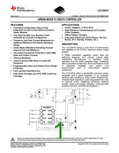
UCC28610
SLUS888C–JANUARY 2009–REVISED SEPTEMBER 2009 ......................................................................................................................................... www.ti.com
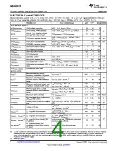
ELECTRICAL CHARACTERISTICS
Unless otherwise stated: VDD = 12 V, VGG=12 V, ZCD = 1 V, FB = 0 V, GND = 0 V, a 0.1-µF capacitor between VDD and
GND, a 0.1-µF capacitor between VGG and GND, RCL = 33.2 kΩ, RMOT = 380 kΩ, –40°C < TA < +125°C, TJ = TA
PARAMETER
VDD and VGG SUPPLY
TEST CONDITIONS
MIN
TYP
MAX UNITS
VGG(OPERATING)
VGG(DISABLED)
VGG voltage, operating
VDD = 14 V, IVGG = 2.0 mA
13
15
14
16
15
VGG voltage, PWM disabled
VDD = 12 V, IVGG = 15 µA, IFB = 350 µA
17
V
Rise in VGG clamping voltage
during UVLO, GM, or Fault
ΔVGG
VGG(DISABLED) – VGG(OPERATING)
1.75
2.00
6
2.15
VGG = VGG(DISABLED) -– 100 mV, VDD =
12 V
IVGG(SREG)
VGG shunt regulator current
10
µA
ΔVGG(SREG)
VGG(LREG)
VGG(LREG, DO)
VDD(ON)
VGG shunt load regulation
VGG LDO regulation voltage
VGG LDO Dropout Voltage
UVLO turn-on threshold
UVLO turn-off threshold
UVLO hysteresis
10 µA ≤ IVGG ≤ 5 mA, IFB = 350 µA
VDD = 20 V, IVGG = – 2 mA
125
13
200
mV
VDD – VGG, VDD = 11 V, IVGG = – 2 mA
1.5
9.7
2
2.5
10.7
8.5
10.2
8
V
VDD(OFF)
7.55
1.9
ΔVDD(UVLO)
IVDD(OPERATING)
IVDD(GM)
2.2
3
2.5
Operating current
VDD = 20 V
2.5
3.7
mA
Idle current between bursts
Current for VDD < UVLO
IFB = 350 µA
550
225
900
310
µA
IVDD(UVLO)
VDD = VDD(ON) – 100 mV, increasing
VDD Switch on resistance, DRV to
VDD
RDS,ON(VDD)
VGG = 12 V, VDD = 7V, IDRV = 50 mA
4
6
10
Ω
VDD(FAULT RESET)
VDD for fault latch reset
5.6
6.4
V
MODULATION
Minimum switching period,
frequency modulation (FM) mode
(1)
(1)
tS(HF)
IFB = 0 µA,
7.125
31
7.5
34
7.875
38
µs
Maximum switching period,
reached at end of FM modulation
range
(1)
(1)
tS(LF)
IFB = IFB, CNR3 – 20 µA,
IFB = 0 µA, RCL = 33. 2 kΩ
IFB = 0 µA, RCL = 100 kΩ
2.85
0.80
0.7
3
0.90
0.85
3.15
1.0
Maximum peak driver current over
amplitude modulation(AM) range
IDRVpk(max)
A
Minimum peak driver current
reached at end of AM modulation
range
IFB, CNR2 + 10 µA, RCL = 33.2 kΩ
1.1
IDRVpk(min)
IFB, CNR2 + 10 µA, RCL = 100 kΩ
0.2
0.33
0.60
0.5
KP
Maximum power constant
For IDRVpk(max) = 3 A
0.54
0.66 W/µH
Minimum peak driver independent
of RCL or AM control
IDRVpk(absmin)
RCL = OPEN
0.3
0.45
220
0.6
A
Leading edge current limit blanking IFB = 0 µA, RCL = 100 kΩ, 1.2-A pull-up on
time
tBLANK(Ilim)
VCL
120
450
ns
DRV
IFB = 0 µA
IFB = (IFB,CNR3 – 20 µA)(1)
2.94
0.95
3
1
3.06
1.05
Voltage of CL pin
V
IFB increasing, tS = tS(LF)
IDRVpk = IDRVpk(max)
,
(2)
IFB,CNR1
IFB range for FM modulation
IFB range for AM modulation
145
35
165
45
195
65
tS = tS(LF), IDRVpk ranges from
IDRVpk(max) to IDRVpk(min)
(2)
(2)
IFB,CNR2 – IFB,CNR1
IFB,CNR3 – IFB,CNR2
µA
IFB range for Green Mode (GM)
modulation
IFB increasing until PWM action is disabled
entering a burst-off state
50
70
90
IFB hysteresis during GM
modulation to enter burst on and
off states
(2)
IFB, GM-HYST
IFB decreasing from above IFB,CNR3
10
25
40
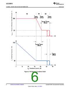
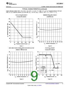
(1) tS sets a minimum switching period. Following the starting edge of a PWM on time, under normal conditions, the next on time is initiated
following the first zero crossing at ZCD after tS. The value of tS is modulated by IFB between a minimum of tS(HF) and a maximum of
tS(LF) In normal operation, tS(HF) sets the maximum operating frequency of the power supply and tS(LF) sets the minimum operating
frequency of the power supply.
(2) Refer to Figure 2.
4
Submit Documentation Feedback
Copyright © 2009, Texas Instruments Incorporated
Product Folder Link(s): UCC28610

 TI [ TEXAS INSTRUMENTS ]