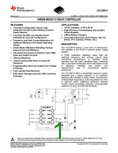
UCC28610
SLUS888C–JANUARY 2009–REVISED SEPTEMBER 2009 ......................................................................................................................................... www.ti.com
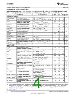
These devices have limited built-in ESD protection. The leads should be shorted together or the device placed in conductive foam
during storage or handling to prevent electrostatic damage to the MOS gates.
ORDERING INFORMATION
OPERATING
TEMPERATURE
RANGE, TA
PACKAGE
LEAD
ORDERABLE PART
NUMBER
PINS
PACKAGE
TRANSPORT MEDIA UNITS
8
8
Plastic Small Outline SOIC
Plastic Dual In-Line PDIP
D
P
Tape and Reel
Tube
2500
50
UCC28610DR
UCC28610P
–40°C to 125°C
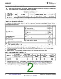
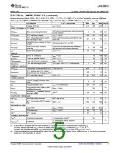
ABSOLUTE MAXIMUM RATINGS(1)
All voltages are with respect to GND, –40°C < TJ = TA < 125°C, all currents are positive into and negative out of the specified
terminal (unless otherwise noted)
UCC28610
–0.5 to +25
–0.5 to +2.0
20
UNIT
VDD
DRV, during conduction
DRV, during non-conduction
VGG(2)
Input voltage range
–0.5 to +16
–0.5 to +7
–0.5 to +1.0
–7 to +10
10
V
(3)
ZCD, MOT, CL
FB(3)
VDD – VGG
(2)
Continuous input current
Input current range
IVGG
mA
A
(3)
IZCD, IMOT, ICL, IFB
–3 to +1
-5
DRV
Peak output current
DRV, pulsed 200ns, 2% duty cycle
–5 to +1.5
–40 to +150
–65 to +150
+260
TJ
Operating junction temperature range
Tstg
Storage temperature range
°C
Lead Temperature (soldering, 10 sec.)
(1) These are stress ratings only. Stress beyond these limits may cause permanent damage to the device. Functional operation of the
device at these or any conditions beyond those indicated under Recommended Operating Conditions is not implied. Exposure to
absolute maximum rated conditions for extended periods of time may affect device reliability
(2) Voltage on VGG is internally clamped. The clamp level varies with operating conditions. In normal use, VGG is current fed with the
voltage internally limited
(3) In normal use, MOT, CL, ZCD, and FB are connected to resistors to GND and internally limited in voltage swing
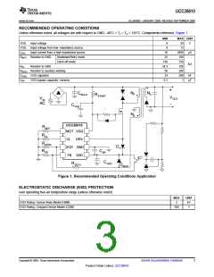
PACKAGE DISSIPATION RATINGS(1) (2)
θJA, THERMAL
IMPEDANCE JUNCTION
TO AMBIENT, NO
θJB, THERMAL
IMPEDANCE JUNCTION
TO BOARD, NO AIRFLOW
(°C/W)(2)
TA = 25°C
POWER RATING
(mW)(3)
TA = 85°C
POWER RATING
(mW)(3)
TB = 85°C
POWER RATING
(mW)(2)(3)
PACKAGE
AIRFLOW (°C/W)(1)
SOIC-8 (D)
PDIP-8 (P)
165
110
55
37
606
909
242
364
730
1080
(1) Tested per JEDEC EIA/JESD51-1. Thermal resistance is a function of board construction and layout. Air flow reducex thermal
resistance. This number is included only as a general guideline; see TI document (SPRA953) IC Package Thermal Metrics.
(2) Thermal resistance to the circuit board is lower. Measured with standard single-sided PCB construction. Board temperature, TB,
measured approximately 1 cm from the lead to board interface. This number is provided only as a general guideline.
(3) Maximum junction temperature, TJ, equal to 125°C
2
Submit Documentation Feedback
Copyright © 2009, Texas Instruments Incorporated
Product Folder Link(s): UCC28610

 TI [ TEXAS INSTRUMENTS ]