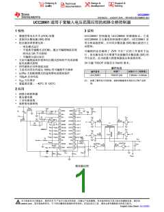
UCC28951
www.ti.com.cn
ZHCSIQ7A –AUGUST 2018 –REVISED DECEMBER 2021
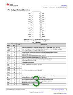
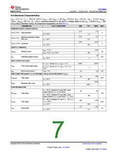
5 Pin Configuration and Functions
1
24
23
22
21
20
19
18
17
16
15
14
13
VREF
EA+
GND
2
VDD
3
EA–
OUTA
OUTB
OUTC
OUTD
OUTE
OUTF
SYNC
CS
4
COMP
SS/EN
DELAB
DELCD
DELEF
TMIN
RT
5
6
7
8
9
10
11
12
RSUM
DCM
ADEL
ADELEF
图5-1. PW Package, 24-Pin TSSOP (Top View)
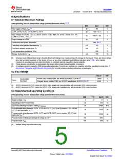
Pin Functions
PIN
TYPE
DESCRIPTION
NAME
ADEL
ADELEF
COMP
CS
NO.
14
13
4
I
Dead-time programming for the primary switches over CS voltage range, tABSET and tCDSET.
I
Delay-time programming between primary side and secondary side switches, tAFSET and tBESET
Error amplifier output and input to the PWM comparator.
Current sense for cycle-by-cycle overcurrent protection and adaptive delay functions.
DCM threshold setting.
.
I/O
15
12
6
I
I
I
I
I
I
I
DCM
DELAB
DELCD
DELEF
EA+
Dead-time delay programming between OUTA and OUTB.
Dead-time delay programming between OUTC and OUTD.
Delay-time programming between OUTA to OUTF, and OUTB to OUTE.
Error amplifier noninverting input.
7
8
2
3
Error amplifier inverting input.
EA–
GND
24
22
21
20
19
18
17
11
10
5
Ground. All signals are referenced to this node.
—
O
O
O
O
O
O
I
OUTA
OUTB
OUTC
OUTD
OUTE
OUTF
RSUM
RT
0.2-A sink and source primary switching output.
Slope compensation programming. Voltage mode or peak current mode setting.
Oscillator frequency set. leader or follower mode setting.
Soft-start programming, device enable and hiccup mode protection circuit.
Synchronization out from leader controller to input of follower controller.
Minimum duty cycle programming in burst mode.
I
SS/EN
SYNC
TMIN
VDD
I
16
9
I/O
I
23
I
Bias supply input.
Copyright © 2023 Texas Instruments Incorporated
Submit Document Feedback
3
Product Folder Links: UCC28951
English Data Sheet: SLUSDB2

 TI [ TEXAS INSTRUMENTS ]