UCC1890
UCC2890
UCC3890
APPLICATION INFORMATION (cont.)
1. When VOUT = 0, the off time is infinite. This feature
provides inherent short circuit protection. However,
to ensure output voltage startup when the output is
not a short, a high value resistor, RS, is placed in
parallel with CT to establish a minimum switching
frequency.
1
Frequency =
TON + TOFF
CT • 3.4V • 0.15 • RON
TON =
VIN – 11V
TOFF
(MAX) =
1.5
•
R
S • T (
C
regions1 and 4
)
2. As VOUT rises above approximately 0.4V, IDCHG is
set by ROFF, and is defined by
CT • 3.4V • ROFF
VOUT − 0.4V
TOFF =
(region 2)
VOUT – 0.4V
IDCHG =
The above equations assume VDD = 9, the voltage
at TON = 11V, the voltage at TOFF = 0.4V.
ROFF
As VOUT increases, IDCHG increases resulting in the
reduction of off time. The frequency of operation in-
creases and VOUT rises quickly to its regulated
value.
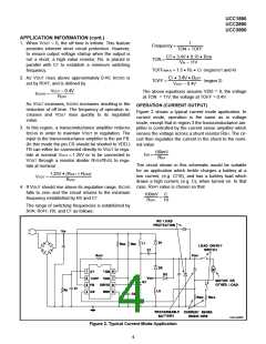
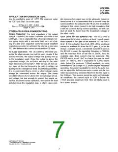
OPERATION (CURRENT OUTPUT)
Figure 2 shows a typical current mode application. In
current mode, operation is the same as in voltage
mode, except that in region 3 the transconductance am-
plifier is controlled by the current sense amplifier which
senses the voltage across a shunt resistor RSH. The cir-
cuit then regulates the current in the shunt to the nomi-
nal value
3. In this region, a transconductance amplifier reduces
IDCHG in order to maintain VOUT in regulation. The
input to the transconductance amplifier is the pin FB.
(In this mode the pin CS should be shorted to VDD.)
FB can either be connected directly to VOUT to regu-
late at nominal VOUT = 1.25V or to be connected to
VOUT through a resistor divider RVS1/RVS2 to regu-
late at nominal
100mV
ISH =
RSH
The circuit shown in this schematic would be suitable
for an application which trickle charges a battery at a
low current, (e.g. C/10), and has a battery load which
draws a high current, (e.g. C), when turned on. In that
case, RSH1 value is chosen so that
1.25V • (RVS1 + RVS2)
VOUT =
RVS2
4. If VOUT should rise above its regulation range, IDCHG
falls to zero and the circuit returns to the minimum
frequency established by RS and CT.
100mV
RSH1
C
10
=
The range of switching frequencies is established by
RON, ROFF, RS, and CT as follows:
UDG-96055
Figure 2. Typical Current Mode Application
4

 TI [ TEXAS INSTRUMENTS ]