UCC28740
www.ti.com
SLUSBF3A –JULY 2013–REVISED JULY 2013
DESIGN PROCEDURE
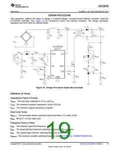
This procedure outlines the steps to design a constant-voltage, constant-current flyback converter using the
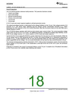
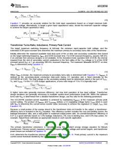
UCC28740 controller. See Figure 19 for component names and network locations. The design procedure
equations use terms that are defined below.
Figure 19. Design Procedure Application Example
Definition of Terms
Capacitance Terms in Farads
CBULK The total input capacitance of CB1 and CB2.
CVDD The minimum required capacitance on the VDD pin.
COUT The minimum output capacitance required.
Duty Cycle Terms
DMAGCC The secondary diode conduction duty-cycle limit in CC mode, 0.425.
DMAX MOSFET on-time duty-cycle.
Frequency Terms in Hertz
fLINE The minimum input-line frequency.
fMAX The target full-load maximum switching frequency of the converter.
fMIN The steady-state minimum switching frequency of the converter.
fSW(min) The minimum possible switching frequency (see ELECTRICAL CHARACTERISTICS).
Copyright © 2013, Texas Instruments Incorporated
Submit Documentation Feedback
19
Product Folder Links: UCC28740

 TI [ TEXAS INSTRUMENTS ]