UCC28180
SLUSBQ5A –NOVEMBER 2013–REVISED NOVEMBER 2013
www.ti.com
Control Logic
The output of the PWM comparator stage is conveyed to the GATE drive stage, subject to control by various
protection functions incorporated into the device. The GATE output duty-cycle may be as high as 98%, but
always has a minimum off-time tOFF_min. Normal duty-cycle operation can be interrupted directly by OVP_H and
PCL. UVLO, ISOP, ICOMMP and OLP/Standby also terminate the GATE output pulse, and further inhibit output
until the SS operation can begin.
Voltage Loop
The outer control loop of the PFC controller is the voltage loop. This loop consists of the PFC output sensing
stage, the voltage error amplifier stage, and the non-linear gain generation.
Output Sensing
A resistor-divider network from the PFC output voltage to GND forms the sensing block for the voltage control
loop. The resistor ratio is determined by the desired output voltage and the internal 5-V regulation reference
voltage.
The very low bias current at the VSENSE input allows the choice of the highest practicable resistor values for
lowest power dissipation and standby current. A small capacitor from VSENSE to GND serves to filter the signal
in a high-noise environment. This filter time constant should generally be less than 100 µs.
Voltage Error Amplifier
The transconductance error amplifier (gmv) generates an output current proportional to the difference between the
voltage feedback signal at VSENSE and the internal 5-V reference. This output current charges or discharges
the compensation network capacitors on the VCOMP pin to establish the proper VCOMP voltage for the system
operating conditions. Proper selection of the compensation network components leads to a stable PFC pre-
regulator over the entire AC-line range and 0% to 100% load range. The total capacitance also determines the
rate-of-rise of the VCOMP voltage at Soft Start, as discussed earlier.
The amplifier output VCOMP is pulled to GND during any fault or standby condition to discharge the
compensation capacitors to an initial zero state. Usually, the large capacitor has a series resistor which delays
complete discharge for their respective time constant (which may be several hundred milliseconds). If VCC bias
voltage is quickly removed after UVLO, the normal discharge transistor on VCOMP loses drive and the large
capacitor could be left with substantial voltage on it, negating the benefit of a subsequent Soft Start. The
UCC28180 incorporates a parallel discharge path which operates without VCC bias, to further discharge the
compensation network after VCC is removed.
If the output voltage perturbations exceed ±5%, and output over-voltage (OVD) or under-voltage (UVD) is
detected, the OVD or UVD function invokes EDR which immediately increases the voltage error amplifier
transconductance to about 280 µS. This higher gain facilitates faster charging or discharging the compensation
capacitors to the new operating level. When output voltage perturbations greater than 107%VREF appear at the
VSENSE input, a 4-kΩ resistor connects VCOMP to ground to quickly reduce VCOMP voltage. When output
voltage perturbations are greater than 109%VREF, the GATE output is shut off until VSENSE drops below 102%
of regulation.
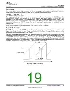
Non-Linear Gain Generation
The voltage at VCOMP is used to set the current amplifier gain and the PWM ramp slope. This voltage is subject
to modification by the SOC function, as discussed earlier.
Together the current gain and the PWM slope adjust to the different system operating conditions (set by the AC-
line voltage and output load level) as VCOMP changes, to provide a low-distortion, high-power-factor, input-
current wave shape following that of the input voltage.
20
Submit Documentation Feedback
Copyright © 2013, Texas Instruments Incorporated
Product Folder Links :UCC28180

 TI [ TEXAS INSTRUMENTS ]