UCC28180
SLUSBQ5A –NOVEMBER 2013–REVISED NOVEMBER 2013
www.ti.com
Current Sense Resistor, RISENSE
The current sense resistor, RISENSE, is sized using the minimum threshold value of Soft Over Current (SOC),
VSOC(min) . To avoid triggering this threshold during normal operation, resulting in a decreased duty-cycle, the
resistor is sized for an overload current of 10% more than the peak inductor current,
VSOC(min)
RISENSE
£
1.1 IL _ PEAK(max)
(1)
Since RISENSE “sees” the average input current, worst-case power dissipation occurs at input low-line when input
current is at its maximum. Power dissipated by the sense resistor is given by:
PRISENSE = I
(
2 R
)
IN_RMS(max)
ISENSE
(2)
Peak current limit (PCL) protection turns off the output driver when the voltage across the sense resistor reaches
the PCL threshold, VPCL. The absolute maximum peak current, IPCL, is given by:
VPCL / 2.5
=
IPCL
RISENSE
(3)
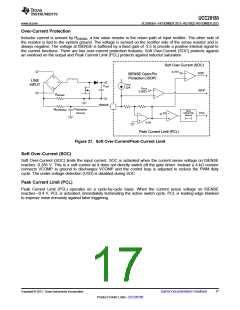
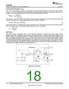
Gate Driver
The GATE output is designed with a current-optimized structure to directly drive large values of total
MOSFET/IGBT gate capacitance at high turn-on and turn-off speeds. An internal clamp limits voltage on the
MOSFET gate to 15.2 V (typical). When VCC voltage is below the UVLO level, the GATE output is held in the off
state. An external gate drive resistor, RGATE, can be used to limit the rise and fall times and dampen ringing
caused by parasitic inductances and capacitances of the gate drive circuit and to reduce EMI. The final value of
the resistor depends upon the parasitic elements associated with the layout and other considerations. A 10-kΩ
resistor close to the gate of the MOSFET/IGBT, between the gate and ground, discharges stray gate capacitance
and helps protect against inadvertent dv/dt-triggered turn-on.
Gate Driver
VCC
7
PWM
FAULT
GATE
GND
OVP_H
8
1
PCL
S
R
Q
Q
Pre-Drive and
Clamp Circuit
Clock
Figure 28. Gate Driver
18
Submit Documentation Feedback
Copyright © 2013, Texas Instruments Incorporated
Product Folder Links :UCC28180

 TI [ TEXAS INSTRUMENTS ]