UCC28180
SLUSBQ5A –NOVEMBER 2013–REVISED NOVEMBER 2013
www.ti.com
DESCRIPTION (CONT.)
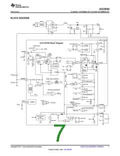
Simple external networks allow for flexible compensation of the current and voltage control loops. In addition,
UCC28180 offers an enhanced dynamic response circuit that is based on the voltage feedback signal to deliver
improved response under fast load transients, both for output over-voltage and under-voltage conditions. An
unique VCOMP discharge circuit provided in UCC28180 is activated whenever the voltage feedback signal
exceeds VOVP_L thus allowing a chance for the control loop to stabilize quickly and avoid encountering the over-
voltage protection function when PWM shut-off can often cause audible noise. Controlled soft start gradually
regulates the input current during start-up and reduces stress on the power switches. Numerous system-level
protection features available in the controller include VCC UVLO, peak current limit, soft over-current, output
open-loop detection, output over-voltage protection and open-pin detection (VISNS). A trimmed internal reference
provides accurate protection thresholds and regulation set-point. The user can control low power standby mode
by pulling the VSENSE pin below 0.82 V.
These devices have limited built-in ESD protection. The leads should be shorted together or the device placed in conductive foam
during storage or handling to prevent electrostatic damage to the MOS gates.
ORDERING INFORMATION
PART NUMBER
PACKAGE
OPERATING TEMPERATURE RANGE, TA
UCC28180D
SOIC 8-Pin (D) Lead (Pb)-Free/Green(1) Lead
(Pb)-Free/Green
–40°C to 125°C
(1) SOIC (D) package is available taped and reeled by adding “R” to the above part number. Reeled quantities are 2,500 devices per reel.
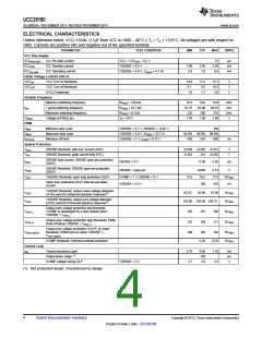
ABSOLUTE MAXIMUM RATINGS(1)
Over operating free-air temperature range, all voltages are with respect to GND (unless otherwise noted). Currents are
positive into and negative out of the specified terminal.
VALUE
MIN
–0.3
–0.3
–24
UNIT
MAX
22
7
Input voltage range
VCC, GATE
V
FREQ, VSENSE, VCOMP, ICOMP
ISENSE
7
Input current range
VSENSE, ISENSE
Operating
–1
1
mA
°C
°C
°C
kV
V
–55
150
150
300
2
Junction temperature, TJ
Lead temperature, TSOL
Storage
–65
Soldering, 10 s
Human Body Model (HBM)
Charged Device Model (CDM)
Electrostatic Discharge (ESD)
Protection
500
(1) Stresses beyond those listed under “absolute maximum ratings” may cause permanent damage to the device. These are stress ratings
only and functional operation of the device at these or any other condition beyond those included under “recommended operating
conditions” is not implied. Exposure to absolute-maximum-rated conditions for extended periods of time may affect device reliability.
2
Submit Documentation Feedback
Copyright © 2013, Texas Instruments Incorporated
Product Folder Links :UCC28180

 TI [ TEXAS INSTRUMENTS ]