UCC28180
www.ti.com
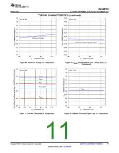
SLUSBQ5A –NOVEMBER 2013–REVISED NOVEMBER 2013
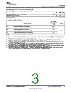
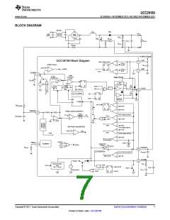
BLOCK DIAGRAM
EMI Filter
LBST
DBST
VOUT
LINE
INPUT
Bridge
Rectifier
–
+
RFB1
QBST
RGATE
CIN
COUT
RLOAD
RFB2
RSENSE
Auxiliary Supply
VCC
UCC28180 Block Diagram
+
+
7
Under voltage lockout
VCCON
11.5V
ICOMP Protection
Q
Q
S
R
CVCC
GND
0.2V
+
ICOMPP
VCCOFF
9.5V
1
UVLO
ICOMP
2
PWM
Comparator
KPC(s)
Current
Amplifier
Gate Driver
+
gmi
CICOMP
S
Q
Q
+
3V
PWM
RAMP
M2
R
FAULT
GAIN
M1, K1
GATE
O
V
P
|
O
L
P
I
OVP_H
Min Off Time
8
S
O
P
Oscillator
H
PCL
S
R
Q
Q
Pre-Drive and
Clamp Circuit
Clock
M2
M1
VCOMP
+
Q
S
OVP_H
RISENSEfilter
5.45V
5.10V
4k
Q
R
+
+
+
ISENSE
Peak Current Limit(PCL)
3
300ns
Leading Edge
Blanking
Over voltage protection
5.35V
1V
PCL
OVP_L
SOC
CISENSEfilter
+
+
-2.5X
EDR
EDR
5.25V
Soft Over Current(SOC)
0.72V
Over voltage detector
4.75V
+
+
SOC
ISOP
Under voltage detector
0.82V
+
OLP/STANDBY
ICOMPP
FREQ
100nA
Oscillator
Voltage Error
Amplifier
ISOP
UVLO
OLP
4
FAULT
5V
+
gmv
RFREQ
VSENSE
CVSENSE
6
5
gmv Enhancement
End of soft start detector
4.9V
+
END OF SS
VCOMP
RCV
Rapid Discharge
when
VCC < VCCOFF
EDR
UVLO
SS
Q
Q
S
R
END OF SS
FAULT
CCV2
FAULT
CCV1
VPRECHARGE
FAULT
Copyright © 2013, Texas Instruments Incorporated
Submit Documentation Feedback
7
Product Folder Links :UCC28180

 TI [ TEXAS INSTRUMENTS ]