UCC27523, UCC27524, UCC27525, UCC27526
SLUSAQ3F –NOVEMBER 2011–REVISED MAY 2013
www.ti.com
ELECTRICAL CHARACTERISTICS (continued)
VDD = 12 V, TA = TJ = -40°C to 140°C, 1-µF capacitor from VDD to GND. Currents are positive into, negative out of the
specified terminal (unless otherwise noted,)
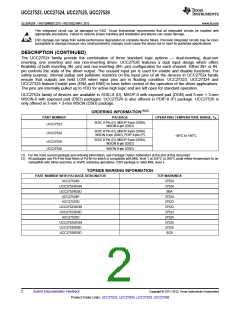
PARAMETER
TEST CONDITION
MIN
TYP
MAX
18
UNITS
(3)
tR
tF
Rise time
CLOAD = 1.8 nF
CLOAD = 1.8 nF
7
6
Fall time(3)
10
Delay matching between 2
channels
INA = INB, OUTA and OUTB at 50% transition
point
tM
1
15
13
13
4
Minimum input pulse width
that changes the output state
ns
tPW
25
23
23
Input to output propagation
tD1, tD2
tD3, tD4
CLOAD = 1.8 nF, 5-V input pulse
CLOAD = 1.8 nF, 5-V enable pulse
6
6
(3)
delay
EN to output propagation
(3)
delay
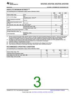
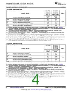
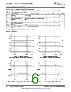
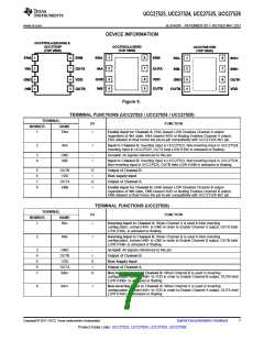
(3) See timing diagrams in Figure 1, Figure 2, Figure 3 and Figure 4
Timing Diagrams
High
Input
Low
High
Input
Low
High
High
Enable
Enable
Low
Low
90%
Output
10%
90%
Output
10%
tD3
tD4
tD3
tD4
UDG-11218
UDG-11217
Figure 1. Enable Function
(For Non-Inverting Input Driver Operation)
Figure 2. Enable Function
(For Inverting Input Driver Operation)
High
Input
Low
High
Input
Low
High
High
Enable
Enable
Low
Low
90%
Output
10%
90%
Output
10%
UDG-11220
tD1
tD2
tD1
tD2
UDG-11219
Figure 3. Non-Inverting Input Driver Operation
Figure 4. Inverting Input Driver Operation
6
Submit Documentation Feedback
Copyright © 2011–2013, Texas Instruments Incorporated
Product Folder Links: UCC27523, UCC27524, UCC27525, UCC27526

 TI [ TEXAS INSTRUMENTS ]