UCC27523, UCC27524, UCC27525, UCC27526
www.ti.com
SLUSAQ3F –NOVEMBER 2011–REVISED MAY 2013
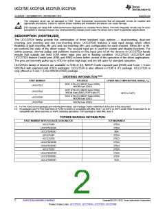
ABSOLUTE MAXIMUM RATINGS(1)(2)
over operating free-air temperature range (unless otherwise noted)
MIN
-0.3 to
MAX
20.0
UNIT
Supply voltage range
OUTA, OUTB voltage
VDD
DC
-0.3 to VDD + 0.3
-2.0 to VDD + 0.3
V
Repetitive pulse < 200 ns(3)
Output continuous source/sink
current
IOUT_DC
0.3
5
A
V
Output pulsed source/sink current
(0.5 µs)
IOUT_pulsed
INA, INB, INA+, INA-, INB+, INB-, ENA, ENB voltage(4)
Human body model, HBM
Charge device model, CDM
-0.3
20
4000
1000
150
ESD(5)
Operating virtual junction temperature, TJ range
Storage temperature range, Tstg
-40
-65
150
°C
Soldering, 10 sec.
Reflow
300
Lead temperature
260
(1) Stresses beyond those listed under absolute maximum ratings may cause permanent damage to the device. These are stress ratings
only and functional operation of the device at these or any other conditions beyond those indicated under recommended operating
conditions is not implied. Exposure to absolute-maximum-rated conditions for extended periods may affect device reliability.
(2) All voltages are with respect to GND unless otherwise noted. Currents are positive into, negative out of the specified terminal. See
Packaging Section of the datasheet for thermal limitations and considerations of packages.
(3) Values are verified by characterization on bench.
(4) The maximum voltage on the Input and Enable pins is not restricted by the voltage on the VDD pin.
(5) These devices are sensitive to electrostatic discharge; follow proper device handling procedures.
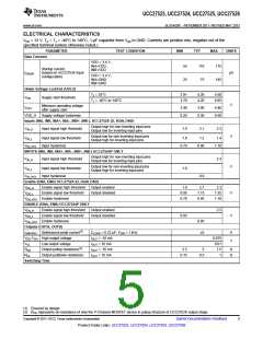
RECOMMENDED OPERATING CONDITIONS
over operating free-air temperature range (unless otherwise noted)
MIN
4.5
-40
0
TYP
MAX
18
UNIT
V
Supply voltage range, VDD
12
Operating junction temperature range
Input voltage, INA, INB, INA+, INA-, INB+, INB-
Enable voltage, ENA and ENB
140
18
°C
V
0
18
Copyright © 2011–2013, Texas Instruments Incorporated
Submit Documentation Feedback
3
Product Folder Links: UCC27523, UCC27524, UCC27525, UCC27526

 TI [ TEXAS INSTRUMENTS ]