UC1526A
UC2526A
UC3526A
APPLICATIONS INFORMATION (cont.)
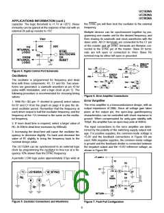
Output Drivers
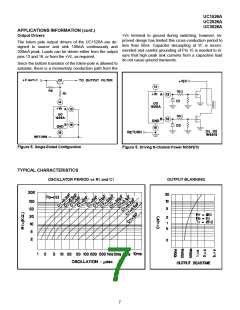
+VC terminal to ground during switching; however, im-
proved design has limited this cross-conduction period to
less than 50ns. Capacitor decoupling at VC is recom-
mended and careful grounding of Pin 15 is needed to in-
sure that high peak sink currents from a capacitive load
do not cause ground transients.
The totem pole output drivers of the UC1526A are de-
signed to source and sink 100mA continuously and
200mA peak. Loads can be driven either from the output
pins 13 and 16, or from the +VC, as required.
Since the bottom transistor of the totem-pole is allowed to
saturate, there is a momentary conduction path from the
Figure 8. Single-Ended Configuration
Figure 9. Driving N-Channel Power MOSFETs
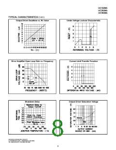
TYPICAL CHARACTERISTICS
OSCILLATOR PERIOD vs RT and CT
OUTPUT BLANKING
7

 TI [ TEXAS INSTRUMENTS ]