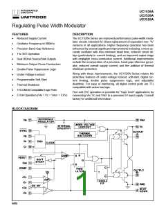
UC1526A
UC2526A
UC3526A
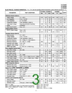
+VIN = 15V, and over operating ambient temperature, unless otherwise specified TA = TJ.
ELECTRICAL CHARACTERISTICS:
UC1526A / UC2526A
UC3526A
TYP
PARAMETER
TEST CONDITIONS
UNITS
MIN
TYP
MAX
MIN
MAX
Reference Section (Note 4)
Output Voltage
TJ = +25°C
4.95
5.00
2
5.05
10
4.90
5.00
2
5.10
15
V
Line Regulation
+VIN = 7 to 35V
IL = 0 to 20mA
mV
mV
mV
V
Load Regulation
5
20
5
20
Temperature Stability
Over Operating TJ (Note 5)
15
5.00
50
15
5.00
50
Total Output Voltage
Range
Over Recommended Operating
Conditions
4.90
25
5.10
4.85
25
5.15
Short Circuit Current
Under-Voltage Lockout
RESET Output Voltage
VREF = 0V
50
100
0.4
50
100
0.4
mA
VREF = 3.8V
VREF = 4.7V
0.2
4.7
0.2
4.8
V
V
2.4
2.4
Oscillator Section (Note 6)
Initial Accuracy
TJ = +25°C
±3
0.5
2
±8
1
±3
0.5
1
±8
1
%
%
Voltage Stability
+VIN = 7 to 35V
Temperature Stability
Minimum Frequency
Maximum Frequency
Sawtooth Peak Voltage
Sawtooth Valley Voltage
SYNC Pulse Width
Over Operating TJ (Note 5)
RT = 150kΩ, CT = 20µF (Note 5)
RT = 2kΩ, CT = 470pF
+VIN = 35V
6
3
%
1
1
Hz
kHz
V
550
0.5
650
0.5
3.0
1.0
1.1
3.5
3.0
1.0
1.1
3.5
+VIN =7V
V
TJ = 25°C, RL = 2.7kΩ to VREF
µs
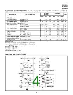
Error Amplifier Section (Note 7)
Input Offset Voltage
Input Bias Current
RS ≤ 2kΩ
2
5
2
10
mV
nA
nA
dB
V
-350 -1000
-350 -2000
Input Offset Current
DC Open Loop Gain
HIGH Output Voltage
LOW Output Voltage
35
72
100
35
72
200
RL ≥ 10MΩ
64
60
VPIN 1 - VPIN 2 ≥ 150mV, ISOURCE = 100µA
VPIN 2 - VPIN 1 ≥ 150mV, ISINK = 100µA
3.6
4.2
0.2
94
3.6
4.2
0.2
94
0.4
0.4
V
Common Mode Rejection RS ≤ 2kΩ
Supply Voltage Rejection +VIN = 12 to 18V
PWM Comparator (Note 6)
70
66
70
66
dB
dB
80
80
Minimum Duty Cycle
Maximum Duty Cycle
VCOMPENSATION = +0.4V
VCOMPENSATION = +3.6V
0
0
%
%
45
49
45
49
Digital Ports (SYNC, SHUTDOWN, and RESET)
HIGH Output Voltage
LOW Output Voltage
HIGH Input Current
LOW Input Current
Shutdown Delay
ISOURCE = 40µA
ISINK = 3.6mA
VIH = +2.4V
2.4
4.0
0.2
2.4
4.0
0.2
V
V
0.4
0.4
-125
-225
160
-200
-360
-125
-225
160
-200
-360
µA
µA
ns
VIL = +0.4V
From Pin 8, TJ = 25°C
Current Limit Comparator (Note 8)
Sense Voltage
RS ≤ 50Ω
90
100
-3
110
-10
80
100
-3
120
-10
mV
µA
ns
Input Bias Current
Shutdown Delay
From pin 7, 100mV Overdrive, TJ = 25°C
260
260
Note 4: IL = 0mA.
Note 7: VCM = 0 to +5.2V
Note 8: VCM = 0 to +12V.
Note 9: VC = +15V.
Note 5: Guaranteed by design, not 100% tested in production.
Note 6: FOSC = 40kHz, (RT = 4.12kΩ ± 1%, CT = 0.01µF± 1%,
RD = 0 Ω).
Note 10:VIN = +35V, RT = 4.12kΩ.
3

 TI [ TEXAS INSTRUMENTS ]