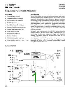
UC1526A
UC2526A
UC3526A
APPLICATIONS INFORMATION
Voltage Reference
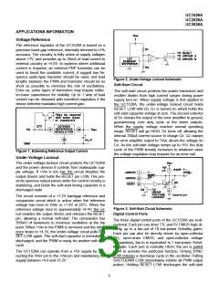
The reference regulator of the UC1526A is based on a
precision band-gap reference, internally trimmed to ±1%
accuracy. The circuitry is fully active at supply voltages
above +7V, and provides up to 20mA of load current to
external circuitry at +5.0V. In systems where additional
current is required, an external PNP transistor can be
used to boost the available current. A rugged low fre-
quency audio-type transistor should be used, and lead
lengths between the PWM and transistor should be as
short as possible to minimize the risk of oscillations.
Even so, some types of transistors may require collec-
tor-base capacitance for stability. Up to 1 amp of load
current can be obtained with excellent regulation if the
device selected maintains high current gain.
Figure 2. Under-Voltage Lockout Schematic
Soft-Start Circuit
The soft-start circuit protects the power transistors and
rectifier diodes from high current surges during power
supply turn-on. When supply voltage is first applied to
the UC1526A, the under-voltage lockout circuit holds
RESET LOW with Q3. Q1 is turned on, which holds the
soft-start capacitor voltage at zero. The second collector
of Q1 clamps the output of the error amplifier to ground,
guaranteeing zero duty cycle at the driver outputs.
When the supply voltage reaches normal operating
range, RESET will go HIGH. Q1 turns off, allowing the
internal 100µA current source to charge CS. Q2 clamps
the error amplifier output to 1VBE above the voltage on
CS. As the soft-start voltage ramps up to +5V, the duty
cycle of the PWM linearly increases to whatever value
the voltage regulation loop requires for an error null.
Figure 1. Extending Reference Output Current
Under-Voltage Lockout
The under-voltage lockout circuit protects the UC1526A
and the power devices it controls from inadequate sup-
ply voltage, If +VIN is too low, the circuit disables the
output drivers and holds the RESET pin LOW. This pre-
vents spurious output pulses while the control circuitry is
stabilizing, and holds the soft-start timing capacitor in a
discharged state.
The circuit consists of a +1.2V bandgap reference and
comparator circuit which is active when the reference
voltage has risen to 3VBE or +1.8V at 25°C. When the
reference voltage rises to approximately +4.4V, the cir-
cuit enables the output drivers and releases the RESET
pin, allowing a normal soft-start. The comparator has
350mV of hysteresis to minimize oscillation at the trip
point. When +VIN to the PWM is removed and the refer-
ence drops to +4.2V, the under-voltage circuit pulls RE-
SET LOW again. The soft-start capacitor is immediately
discharged, and the PWM is ready for another soft-start
cycle.
Figure 3. Soft-Start Circuit Schematic
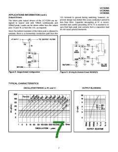
Digital Control Ports
The three digital control ports of the UC1526A are bi-di-
rectional. Each pin can drive TTL and 5V CMOS logic di-
rectly, up to a fan-out of 10 low-power Schottky gates.
Each pin can also be directly driven by open-collector
TTL, open-drain CMOS, and open-collector voltage
comparators; fan-in is equivalent to 1 low-power Schot-
tky gate. Each port is normally HIGH; the pin is pulled
LOW to activate the particular function. Driving SYNC
LOW initiates a discharge cycle in the oscillator. Pulling
SHUTDOWN LOW immediately inhibits all PWM output
pulses. Holding RESET LOW discharges the soft-start
The UC1526A can operate from a +5V supply by con-
necting the VREF pin to the +VIN pin and maintaining the
supply between +4.8 and +5.2V.
5

 TI [ TEXAS INSTRUMENTS ]