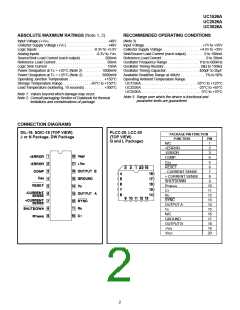
UC1526A
UC2526A
UC3526A
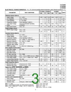
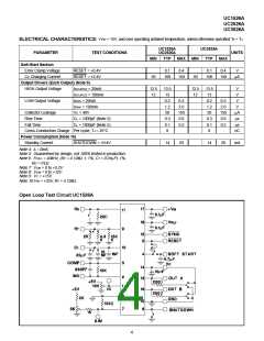
APPLICATIONS INFORMATION (cont.)
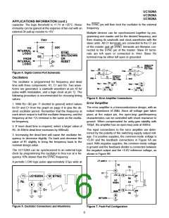
capacitor. The logic threshold is +1.1V at +25°C. Noise
immunity can be gained at the expense of fan-out with an
external 2k pull-up resistor to +5V.
the SYNC pin will then lock the oscillator to the external
frequency.
Multiple devices can be synchronized together by pro-
gramming one master unit for the desired frequency, and
then sharing its sawtooth and clock waveforms with the
slave units. All CT terminals are connected to the CT pin
of the master and all SYNC terminals are likewise con-
nected to the SYNC pin of the master. Slave RT termi-
nals are left open or connected to VREF. Slave RD
terminal may be either left open or grounded.
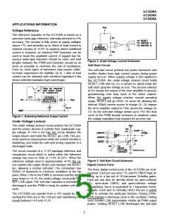
Figure 4. Digital Control Port Schematic
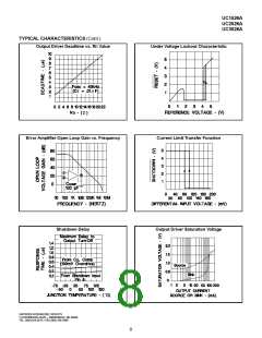
Oscillators
The oscillator is programmed for frequency and dead
time with three components: RT, CT and RD. Two wave-
forms are generated: a sawtooth waveform at pin 10 for
pulse width modulation, and a logic clock at pin 12. The
following procedure is recommended for choosing timing
values:
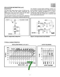
Figure 6. Error Amplifier Connections
Error Amplifier
1. With RD= 0Ω (pin 11 shorted to ground) select values
for RT and CT from the graph on page 4 to give the de-
sired oscillator period. Remember that the frequency at
each driver output is half the oscillator frequency, and the
frequency at the +VC terminal is the same as the oscilla-
tor frequency.
The error amplifier is a transconductance design, with an
output impedance of 2MΩ. Since all voltage gain takes
place at the output pin, the open-loop gain/frequency
characteristics can be controlled with shunt reactance to
ground. When compensated for unity-gain stability with
100pF, the amplifier has an open-loop pole at 800Hz.
2. If more dead time is required, select a larger value of
The input connections to the error amplifier are deter-
mined by the polarity of the switching supply output volt-
age. For positive supplies, the common-mode voltage is
+5.0V and the feedback connections in Figure 6A are
used. With negative supplies, the common-mode voltage
is ground and the feedback divider is connected between
the negative output and the +5.0V reference voltage, as
shown in Figure 6B.
RD. At 40kHz dead time increases by 400ns/Ω.
3. Increasing the dead time will cause the oscillator fre-
quency to decrease slightly. Go back and decrease the
value of RT slightly to bring the frequency back to the
nominal design value.
The UC1526A can be synchronized to an external logic
clock by programming the oscillator to free-run at a fre-
quency 10% slower than the SYNC frequency.
A periodic LOW logic pulse approximately 0.5µs wide at
Figure 5. Oscillator Connections and Waveforms
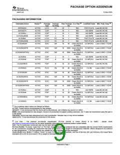
Figure 7. Push-Pull Configuration
6

 TI [ TEXAS INSTRUMENTS ]