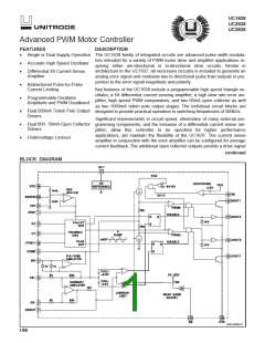
UC1638
UC2638
UC3638
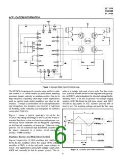
APPLICATION INFORMATION (cont.)
remains constant, preventing low frequency oscillator With integral compensation, the average current loop
modulation in the presence of line voltage changes.
will have very high DC gain, resulting in effectively no
average DC motor current error. For stability purposes,
the high frequency gain of the voltage error amplifier
must be designed such that magnitude of the slope of
the error amplifier output (COMP) must be less than or
equal to the magnitude of the slope of the triangle wave-
form.
Output Drivers
The output driver section provides separate output driv-
ers for high and low side drive of both PWM signals. For
many applications, the 500mA peak output current ca-
pability of the low side drivers (AOUT2 and BOUT2) is
sufficient to directly connect to the appropriate low side
MOSFETs of the H-bridge. A current limiting gate resis-
tor may be used to control switching time if high levels of
dv/dt or di/dt are expected at the drains of the MOS-
FETs. If more current drive capability is required, the
PWM drive signals can be buffered with bipolar transis-
tors.
If RS1 = RS2 = RS, the DC gain of the current control
loop can be calculated as:
IMOTOR
ICMD
RG2
=
5 • RG1• RS
If the UC3638 is set up in a simple velocity or position
control loop, the feedback voltage (speed or position) is
summed directly into the voltage error amplifier, and the
current sense amplifier is only used for peak current
limit control. The motor can also be replaced by another
high power device, such as an audio speaker, and the
same type of amplifier can be used. In the case of audio
however, a higher switching frequency will probably be
desired to prevent switching noise from infiltrating the
audio frequency range.
The open collector high side drivers (AOUT1 and
BOUT1) are designed to control high side P-channel
MOSFETs. Depending on voltage and speed require-
ments, the driver stage can be simplified from the one
shown on Figure 1. If high side N-channel MOSFETs
are desired, a boot strap or charge pump based drive
circuit can be used as long as 100% duty cycle opera-
tion is not required.
Average Current Control
UVLO and Shutdown
The UC3638 incorporates all of the necessary features
for precise average current loop control of a DC motor.
In the circuit shown in Figure 1, motor current is sensed
differentially across two current sense resistors.By using
two current sense resistors both the current sourced
from the motor voltage supply (Vm) and the flyback cur-
rent are sensed in the correct polarity to provide true
torque control. If only one current sensed resistor is
used, the flyback current will circulate through the body
diodes of the lower MOSFETs and bypass the current
sense resistor. The result will be a duty cycle dependent
error term in the loop torque control function. In order to
prevent high frequency spikes from contributing exces-
sive error to the current control loop, the switching
speed of the MOSFETs must be controlled so that sig-
nificant transient current spikes do not couple across
the drain to source capacitance of the MOSFETs.
The UC3638 contains undervoltage lockout (UVLO) cir-
cuitry to prevent unwanted bridge turn-on before suffi-
cient supply voltage is available. The open collector
drivers (AOUT1 and BOUT1) are held off (no sink cur-
rent) and the totem pole drivers (AOUT 2 and BOUT2)
are pulled low until the voltage between VCC and VEE
reaches 9V typical. The UVLO circuitry becomes active
at approximately 1V, and before this level the totem pole
drivers are held low with passive pull down resistors.
The shutdown pin holds the output drivers in their inac-
tive state unless it is pulled 2.5V below VCC. An open
collector gate or transistor can be used as an external
enable signal, or a turn-on voltage higher than UVLO
can be programmed with a resistive divider. In the case
of Figure 1, the turn on voltage VSTART can be calcu-
lated as:
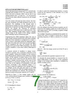
The X5 current amplifier multiplies the current signal by
a factor of 5 and feeds the average current signal into
the error amplifier. A window comparator detects if the
peak current signal at the output of the current amplifier
has a magnitude greater than 2.5V in either polarity and
provides pulse-by-pulse peak current limiting. The loop
should be designed so that peak motor current never
reaches this level during normal operation.
2.5 • (R1+R2)
VSTART =
R1
If a delayed start is desired, a capacitor can be placed
in parallel with R1 to slow down the change in voltage at
the shutdown pin, and thus provide a user programma-
ble startup time.
UNITRODE CORPORATION
7 CONTINENTAL BLVD. • MERRIMACK, NH 03054
TEL. (603) 424-2410 • FAX (603) 424-3460
8

 TI [ TEXAS INSTRUMENTS ]