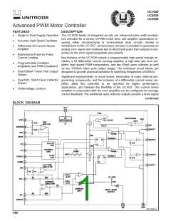
UC1638
UC2638
UC3638
Unless otherwise specified; VCC = 15V, VEE =–15V, CT = 680pF, RT = 3k,
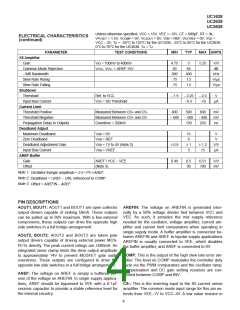
ELECTRICAL CHARACTERISTICS
(continued)
VPVSET = 1.5V, VCOMP = 0V, VCSOUT = 0V, VDB = REF, VEXTREF = 0V, VSD =
VCC – 3V, TA = −55°C to 125°C for the UC1638, −25°C to 85°C for the UC2638,
0°C to 70°C for the UC3638. TA = TJ.
PARAMETER
X5 Amplifier
TEST CONDITIONS
MIN
TYP
MAX UNITS
Gain
VID = 100mV to 400mV
4.75
50
5
5.25
V/V
dB
±
Common Mode Rejection
−3dB Bandwidth
Slew Rate Rising
Slew Rate Falling
Shutdown
VCS+, VCS− = AREF 5V
65
300
.75
.75
400
1.5
1.5
kHz
V/µs
V/µs
Threshold
Ref. to VCC
− 1.9
− 2.25
−0.5
− 2.5
−10
V
Input Bias Current
Current Limit
VSD = SD Threshold
µA
Threshold Positive
Threshold Negative
Propagation Delay to Outputs
Deadband Adjust
Maximum Deadband
Zero Deadband
Deadband Adjustment Gain
Input Bias Current
AREF Buffer
Measured Between CS+ and CS-
Measured Between CS+ and CS-
Overdrive = 200mV
400
500
− 500
150
600
– 400
250
mV
mV
ns
– 600
±
VDB = 0V
5
1
V
V
VDB = REF
0
±
±
±
VDB = 1V to 4V (Note 2)
VDB = VREF
0.9
1.2
V/V
µA
3
15
Gain
AREF / VCC − VEE
0.49
0.5
30
0.51
100
V/V
mV
Offset
(Note 3)
Note 1:
±
Oscillator triangle amplitude = 2.5 • PV AREF.
Note 2:
Note 3:
±
Deadband = (REF − DB), referenced to COMP.
Offset = AREFIN − AREF.
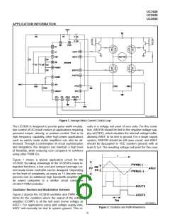
PIN DESCRIPTIONS
AOUT1, BOUT1: AOUT1 and BOUT1 are open collector AREFIN: The voltage on AREFIN is generated inter-
output drivers capable of sinking 50mA. These outputs nally by a 50% voltage divider tied between VCC and
can be pulled up to 60V maximum. With a few external VEE. As such, it provides the mid supply reference
components, these outputs can drive the opposite high needed for the oscillator, voltage amplifier, current am-
side switches in a full bridge arrangement.
plifier and current limit comparators when operating in
single supply mode. A buffer amplifier is connected be-
tween AREFIN and AREF. In bipolar supply applications
AREFIN is usually connected to VEE, which disables
the buffer amplifier, and AREF is connected to 0V.
AOUT2, BOUT2: AOUT2 and BOUT2 are totem pole
output drivers capable of driving external power MOS-
FETs directly. The peak current ratings are 500mA. An
integrated zener clamp limits the drive output amplitude
±
to approximately 14V to prevent MOSFET gate oxide COMP: This is the output of the high slew rate error am-
overstress. These outputs are configured to drive the plifier. The level on COMP modulates the controller duty
opposite low side switches in a full bridge arrangement.
cycle via the PWM comparators and the oscillator ramp.
Compensation and DC gain setting resistors are con-
nected between COMP and INV.
AREF: The voltage on AREF is simply a buffered ver-
sion of the voltage on AREFIN. In single supply applica-
tions, AREF should be bypassed to VEE with a 0.1µF CS-: This is the inverting input to the X5 current sense
ceramic capacitor to provide a stable reference level for amplifier. The common mode input range for this pin ex-
the internal circuitry.
tends from VEE−1V to VCC−4V. A low value resistor in
4

 TI [ TEXAS INSTRUMENTS ]