UC1638
UC2638
UC3638
PIN DESCRIPTIONS (cont.)
series with the source or emitter of the low side switch in ground. Internal level shifting circuitry gives the option of
the full bridge develops the signal that is applied to this tying this pin to VEE, or the system ground in split sup-
ply applications.
±
pin. At differential inputs of 500mV typical (referenced
to CS+)the controller reaches the current limit level,
which truncates the output pulse.
PVSET: A DC voltage on PVSET programs the upper
and lower thresholds for the oscillator by the following
relationship:
CS+: This is the non-inverting input to the X5 current
sense amplifier. The common mode input range for this
pin extends from VEE−1V to VCC−4V. The characteris-
tics for this pin are identical to CS-.
VPK − VVLY = 5 • VPVSET.
The input voltage range on PVSET is 0.5V to REF.
CSOUT: This is the output of the X5 current sense am-
REF: REF is the output of the precision reference. The
output is capable of supplying 15mA to peripheral cir-
cuitry and is internally short circuit current limited. By-
pass REF to VEE with a 0.1µF ceramic capacitor for
best performance.
±
plifier. Voltage levels greater than 2.5V referenced to
AREF will cause the device to enter current limit. An in-
ternal 100 ohm resistor between the amplifier output
and CSOUT is provided to create a high frequency
noise filter with an external capacitor to VEE. When
used for average current feedback, CSOUT is summed
into INV.
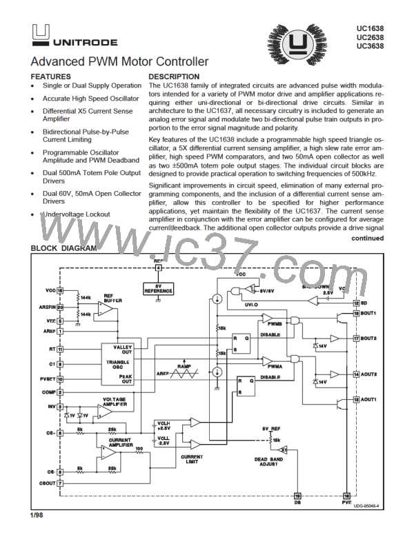
RT: A single resistor from RT to VEE sets the charging
and discharging currents for the triangle oscillator. The
actual charge and discharge is 2X the current pro-
grammed by RT and PVSET. For best performance the
current out of RT should be limited to 1mA. The voltage
level on the RT pin is a buffered version of the PVSET
pin voltage. Therefore, if the PVSET voltage divider is
tied between VCC and VEE to incorporate line feedfor-
ward, the triangle waveform frequency will remain con-
stant.
CT: A capacitor from CT to VEE will set the triangle os-
cillator frequency according to the following equation:
1
F =
5 • RT • CT
The waveform on CT is symmetrical about the voltage
on AREF and is applied internally to the inputs of hte
PWM comparators. Use a high quality ceramic capacitor
with low ESL and ESR for best results. A minimum CT
value of 200 pF insures good accuracy and less suscep-
tibility to circuit layout parasitics. The oscilator and PWM
are designed to provide practical operation to 500kHz.
SD: A voltage on SD within 2.5V (typical) of VCC will
cause the UC3638 to enter a UVLO condition which dis-
ables all of the driver outputs. With an external voltage
divider across VCC and VEE, and a capacitor between
SD and VCC, a delayed turn-on characteristic can be
generated. Since the 2.5V threshold is temperature sta-
bilized it can also be used as a higher UVLO threshold
for applications which require a starting voltage higher
than the internal 9V UVLO threshold.
DB: This high impedance input programs output pulse
train deadtime. A stable DC voltage between 0V and
REF will set a bi-directional deadband centered about
the level on COMP. The deadband level is equal to: 5V −
±
VDB. That is, 1V on DB will program 4V of deadband
centered about the COMP pin level. A convenient
method for generating the programming level is a volt-
age divider tap off of REF.
VEE: All voltages are measured with respect to this pin.
All bypass capacitors and timing components except
those listed under the PVE section should be connected
to this pin. Component leads should be as short and di-
rect as possible. VEE is generally connected to the most
negative voltage supply in the system. In single supply
applications, VEE is tied to the system ground.
INV: This is the inverting input to the Voltage amplifier.
The common mode input range for this pin extends from
VEE+2V to VCC−1V. It can be tied to a command signal
generated by a rate feedback element or to a position
control signal. In average current feedback applications,
this input is tied to the output of the X5 current sensing
amplifier (CSOUT).
VCC: Positive supply rail for the IC. Bypass this pin to
VEE and PVE with 0.1 to 1µF low ESL, ESR ceramic
capacitor(s). The maximum voltage for VCC is 40V ref-
PVE: This is the high current ground for the IC. The ex- erenced to VEE. The turn on voltage level on VCC is 9V
ternal MOSFET driver transistors are referenced to this with 1V of hysteresis.
5

 TI [ TEXAS INSTRUMENTS ]