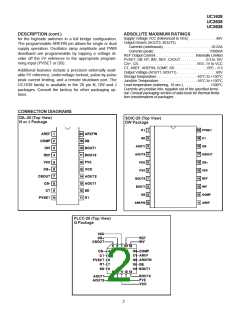
UC1638
UC2638
UC3638
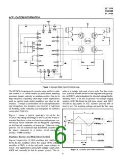
APPLICATION INFORMATION (cont.)
will be half way between ground and VCC, and will auto- In order to select the programming resistors, a source
matically track changes in VCC. For cases where a dif- current for the reference is first selected. For a 1mA
ferent null point is desired, AREF can be tied to any source current:
voltage between VEE + 2V and VCC − 2V. Of course the
user must also allow sufficient headroom for the triangle
waveform.
5
5
R3 + R4 + R5 =
=
= 5k
ISOURCE 1mA
1V
5 - VDB
R3 =
=
= 1k
ISOURCE 1mA
VDB - VPVSET 4V - 1.2V
Once the system null point has been chosen, the trian-
gle wave amplitude and PWM deadband must be pro-
grammed. The amplitude of the triangle wave is
determined by trading off noise immunity and gain re-
quirements. In general, the larger the triangle wave am-
plitude, the greater the immunity to premature
termination of PWM pulses due to switching noise. How-
ever, high amplitude triangle waves require a greater
voltage swing at the output of the voltage amplifier
which ultimately reduces forward loop gain.
R4 =
=
= 2.8k
ISOURCE
1mA
R5 = 5k − 1k − 2.8k = 1.2k
All of the voltages described by these equations are ref-
erenced to the negative supply rail. In other words, for a
split supply system, VREF is actually a negative voltage
referenced to ground.
The oscillator frequency is programmed by proper se-
lection of RT and CT. If 220pF is chosen for CT, and an
operating frequency of 30kHz is desired, RT is chosen
by:
Programming the PWM deadband allows the user to
trade off gain linearity requirements with power amplifier
efficiency. If the modulator is configured as in Figure 1,
motor current is alternately pulsed by diagonally oppo-
site drive FETs when the servo loop is at null. By adjust-
ing the deadband, the user can program the offset
voltage at the input of the PWM comparators. This offset
results in deadtime, or time when neither PWM signal is
active.
1
F =
5 • RT • CT
1
30kHz =
5 • 220pF • RT
RT = 30k
With RT = 30k, the charge current out of the RT pin is
limited to
A minimum amount of deadtime is always recom-
mended to provide cross conduction protection at the
power amplifier. Setting the deadtime to this minimum
level will provide the maximum motor stiffness or holding
torque, at the expense of power losses in the output
stage. These losses result from the fact that the power
amplifier is always sourcing motor current, even at null.
As deadtime is increased, amplifier losses at null be-
come less, at the expense of nonlinearity in the gain
function. Eventually, if the deadband voltage is in-
creased to equal the amplitude of the triangle wave, er-
ror voltages at the null point will result in no PWM
pulsing, or a dead zone. After the triangle waveform am-
plitude and deadband are selected, the operating fre-
quency is easily set by proper selection of CT and RT.
1.2V
= 40µA,
30k
which is well within the specified maximum of 1mA.
To calculate the actual deadtime or minimum time be-
tween PWM pulses (TDB), the ratio of the deadband
voltage to the triangle wave amplitude is multiplied by
half the oscillator period:
DB
1
f
TDB =
•
VPK - VVLY
5 - VDB
=
=
• (5 • RT • CT)
5 • VPVSET
(5 - VDB) • RT • CT
VPVSET
Referring to Figure 1, if the voltage supply rails are
For this example the deadtime is:
±
15V, and the desired triangle wave oscillator amplitude
1• 30k • 220pF
TDB =
= 5.5µsec
is 6V p-p, PVSET is set by:
1.2
VPK − VVLY = 5 • VPVSET
If voltage feedforward is desired, PVSET should be de-
rived off of the supply rails instead of VREF. This way
changes in the supply voltage will linearly regulate the
modulator gain, which decreases control loop suscepti-
bility to line voltage variations. Since the voltage on the
RT pin is a buffered version of PVSET, charge current
tracks oscillator amplitude, and therefore the frequency
6
VPVSET = = 1.2V
5
If 1V of deadband is chosen:
5 − VDB = 1V
VDB = 4V
7

 TI [ TEXAS INSTRUMENTS ]