TUSB1310A
SLLSE32D–NOVEMBER 2010–REVISED MAY 2011
www.ti.com
List of Figures
1-1
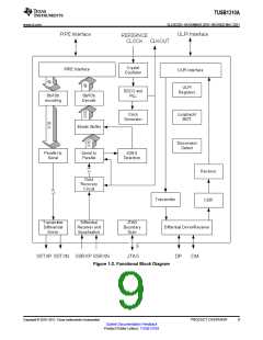
1-2
3-1
5-1
5-2
5-3
5-4
6-1
6-2
6-3
6-4
6-5
Typical Application.................................................................................................................
Functional Block Diagram ........................................................................................................
8
9
Power-Up Sequence............................................................................................................. 19
Analog Pin Connections......................................................................................................... 28
USB Standard-A Connector Pin Connection ................................................................................. 29
USB Standard-B Connector Pin Connection ................................................................................. 29
Typical Crystal Connections .................................................................................................... 30
Power Up and Reset Timing.................................................................................................... 34
PIPE Transmit Timing ........................................................................................................... 34
PIPE Receive Timing ............................................................................................................ 35
ULPI Transmit Timing............................................................................................................ 36
ULPI Receive Timing ............................................................................................................ 36
4
List of Figures
Copyright © 2010–2011, Texas Instruments Incorporated

 TI [ TEXAS INSTRUMENTS ]