TUSB1310A
SLLSE32D–NOVEMBER 2010–REVISED MAY 2011
www.ti.com
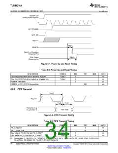
VDD1P8 and
Analog Power Supplies
XI
OUT_ENABLE
ULPI_DIR
VDD1P1
Tcfgin1
RESETN
Latch-In of Hardware
Strapping Pins
Tcfgin2
Drive Output
Strapping pins
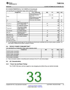
Figure 6-1. Power Up and Reset Timing
Table 6-1. Power Up and Reset Timing
DESCRIPTION
Hardware configuration latch-in time from RESETN
Time from RESETN to driver outputs on strapping pins
RESETN pulse width
SYMBOL
Tcfgin1
MIN
0
TYP
MAX
UNITS
ns
Tcfgin2
0
ns
1
µs
RESETN to PHY_STATUS de-assertion
300
µs
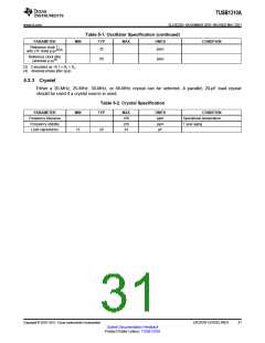
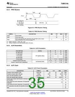
6.5.2 PIPE Transmit
Figure 6-2. PIPE Transmit Timing
Table 6-2. PIPE Transmit Timing
DESCRIPTION
SYMBOL
Tcyc2
Tdty2
MIN
TYP
4
MAX
UNITS
ns
TX_CLK period
TX_CLK duty cycle
50
%
Data setup to TX_CLK rise and TX_CLK fall(1)
Data hold to TX_CLK rise and TX_CLK fall(1)
Tsu2
1
0
ns
Thd2
ns
(1) This includes TX_DATA15-0, TX_DATAK1-0, TX_ONESZEROS, RATE, TX_DEEMPTH, TX_DETRX_LPBK, TX_ELECIDLE,
TX_MARGIN, TX_SWING, RX_POLARITY, POWER_DOWN1-0.
34
ELECTRICAL SPECIFICATIONS
Copyright © 2010–2011, Texas Instruments Incorporated
Submit Documentation Feedback
Product Folder Link(s): TUSB1310A

 TI [ TEXAS INSTRUMENTS ]