TUSB1310A
www.ti.com
SLLSE32D–NOVEMBER 2010–REVISED MAY 2011
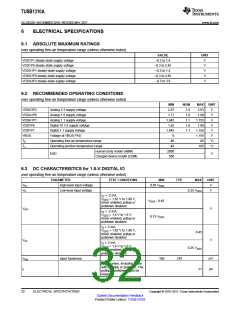
DC CHARACTERISTICS for 1.8-V DIGITAL IO (continued)
over operating free-air temperature range (unless otherwise noted)
PARAMETER
TEST CONDITIONS
MIN
TYP
MAX
UNIT
Receiver/pullup only, pullup
enabled (not inhibited),
VPAD = 0 V
-47 to -169
II(PUon)
µA
Receiver/pullup only, pullup
enabled (not inhibited)
–100
IOZ
IZ
Driver only, driver disabled
±20
±20
µA
µA
(1)
See
SSTXP/SSTXN differential
p-p TX voltage swing
VTX_DIFF_SS
RTX_DIFF_DC
0.8
72
1.2
V
DC differential impedance
120
Ω
The amount of voltage
change allowed during
receiver detection
VTX_RCV_DET
0.6
V
CAC_COUPLING
RRX_DC
AC coupling capacitor
75
18
200
30
nF
Receiver DC common
mode impedance
Ω
RRX_DIFF_DC
DC differential impedance
LFPS detect threshold
72
120
300
100
10
Ω
VRX_LFPS_DET
VCM_AC_LFPS
100
mV
mV
mV
mV
VCM_LFPS_active
VTX_DIFF_PP_LFPS
800
1200
(1) IZ is the total leakage current through the PAD connection of a driver/receiver combination that may include a pullup or pulldown. The
driver output is disabled and the pullup or pulldown is inhibited.
6.4 DEVICE POWER CONSUMPTION(1)
over operating free-air temperature range (unless otherwise noted)
PARAMETER
MIN
TYP
13
MAX
UNIT
mW
mW
mW
mW
mW
VDDA3P3 power consumption
VDDA1P8 power consumption
VDDA1P1 power consumption
VDD1P1 power consumption
VDD1P8 power consumption
77
118
98
128
(1) Power consumption condition is transmitting and/or receiving (in U0) at 25°C and nominal voltages.
6.5 AC Characteristics
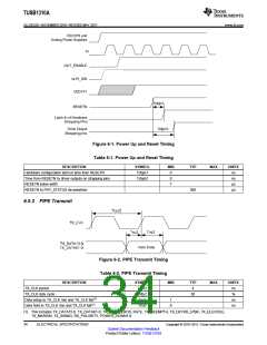
6.5.1 Power Up and Reset Timing
The TUSB1310A does not drive signals on any strapping pins before they are latched internally.
Copyright © 2010–2011, Texas Instruments Incorporated
ELECTRICAL SPECIFICATIONS
33
Submit Documentation Feedback
Product Folder Link(s): TUSB1310A

 TI [ TEXAS INSTRUMENTS ]