TPS7H5005-SEP, TPS7H5006-SEP, TPS7H5007-SEP, TPS7H5008-SEP
SLVSGG1 – FEBRUARY 2022
www.ti.com
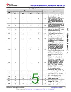
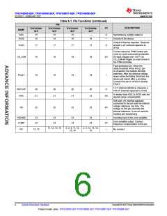
Table 6-1. Pin Functions (continued)
PIN
I/O
DESCRIPTION
TPS7H5005-
SEP
TPS7H5006-
SEP
TPS7H5007-
SEP
TPS7H5008-
SEP
NAME
SRA
15
16
15
16
15
16
—
O
Synchronous rectifier output A.
Ground of the device.
AVSS
16
—
Output of internal regulator. Requires
at least 1-μF external capacitor to
AVSS.
VLDO
17
17
17
17
18
O
Current sense for PWM control and
cycle-by-cycle overcurrent protection.
An input voltage over 1.05 V on
CS_ILIM will trigger an overcurrent in
the PWM controller.
CS_ILIM
18
18
18
I/O
Fault protection pin. When the
rising threshold of the FAULT pin
is exceeded, the outputs will stop
switching. After the external voltage
drops below the falling threshold, the
device will restart after a set delay.
Connect this pin to AVSS to disable
FAULT.
FAULT
19
19
19
19
I
1.2-V internal reference. Requires a
470-nF external capacitor to AVSS.
REFCAP
RSC
20
21
20
21
20
21
20
21
O
A resistor from RSC to AVSS sets the
desired slope compensation.
I/O
Soft start. An external capacitor
connected to this pin sets the internal
voltage reference rise time. The
voltage on this pin overrides the
internal reference. It can be used for
tracking and sequencing.
SS
22
22
22
22
I/O
VSENSE
COMP
23
24
23
24
23
24
23
24
I
Inverting input of the error amplifier.
Error amplifier output. Connect
frequency compensation to this pin.
I/O
11, 12, 13, 14
2, 3, 4, 11, 12,
13, 14
2, 3, 12, 13, 14,
15
NC
12, 13
—
No connect.
Copyright © 2022 Texas Instruments Incorporated
6
Submit Document Feedback
Product Folder Links: TPS7H5005-SEP TPS7H5006-SEP TPS7H5007-SEP TPS7H5008-SEP

 TI [ TEXAS INSTRUMENTS ]