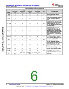
TPS7H5005-SEP, TPS7H5006-SEP, TPS7H5007-SEP, TPS7H5008-SEP
SLVSGG1 – FEBRUARY 2022
www.ti.com
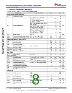
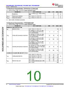
7.5 Electrical Characteristics: All Devices (continued)
TJ = –55°C to 125°C, VIN = 4 V to 14 V (unless otherwise noted)
PARAMETER
TEST CONDITIONS
MIN
TYP
MAX UNIT
RLOAD = 50 kΩ, CLOAD = 100 pF, 10% to
90%
Rise/fall time
10
17
ns
RSRC_P
RSINK_P
Output source resistance
Output sink resistance
IOUT = 20 mA, 5 V ≤ VIN ≤ 14 V
IOUT = 20 mA, 5 V ≤ VIN ≤ 14 V
15
15
Ω
Ω
(1) Bench verified. Not tested in production.
7.6 Electrical Characteristics: TPS7H5005-SEP
TJ = –55°C to 125°C, VIN = 4 V to 14 V (unless otherwise noted)
PARAMETER
TEST CONDITIONS
MIN
TYP
MAX UNIT
MINIMUM ON-TIME AND DEAD TIME
tMIN
Minimum on-time
LEB = 10 kΩ, 5 V ≤ VIN ≤ 14 V
85
11
ns
PS = floating, 5 V ≤ VIN ≤ 14 V, 90%
of OUTx falling to 10% of SRx rising,
OUTx and SRx floating
5
43
85
5
8
50
PS = 49.9 kΩ, 5 V ≤ VIN ≤ 14 V, 90%
TDPS
Primary off to secondary on dead time of OUTx falling to 10% of SRx rising,
OUTx and SRx floating
55
110
11
ns
PS = 107 kΩ, 5 V ≤ VIN ≤ 14 V, 90%
of OUTx falling to 10% of SRx rising,
OUTx and SRx floating
100
8
SP = floating, 5 V ≤ VIN ≤ 14 V, 90%
of SRx falling to 10% of OUTx rising,
OUTx and SRx floating
SP = 49.9 kΩ, 5 V ≤ VIN ≤ 14 V, 90% of
Secondary off to primary on dead time SRx falling to 10% of OUTx rising edge,
OUTx and SRx floating
TDSP
43
85
50
55
ns
SP = 107 kΩ, 5 V ≤ VIN ≤ 14 V, 90%
of SRx falling to 10% of OUTx rising,
OUTx and SRx floating
100
110
LEADING EDGE BLANK TIME AND DUTY CYCLE
LEB = 10 kΩ, 5 V ≤ VIN ≤ 14 V
LEB = 49.9 kΩ, 5 V ≤ VIN ≤ 14 V
LEB = 110 kΩ, 5 V ≤ VIN ≤ 14 V
DCL = AVSS
12
45
85
45
70
15
50
19
55
TLEB
Leading edge blank time
Maximum duty cycle
ns
%
100
48
110
50
DMAX
DCL = floating, clock duty cycle = 50%
DCL = VLDO
75
80
100
Copyright © 2022 Texas Instruments Incorporated
10
Submit Document Feedback
Product Folder Links: TPS7H5005-SEP TPS7H5006-SEP TPS7H5007-SEP TPS7H5008-SEP

 TI [ TEXAS INSTRUMENTS ]