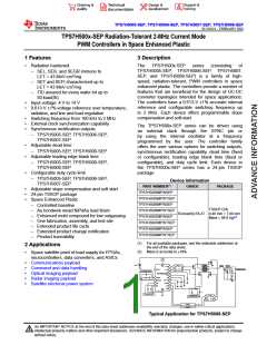
TPS7H5005-SEP, TPS7H5006-SEP, TPS7H5007-SEP, TPS7H5008-SEP
www.ti.com
NAME
SLVSGG1 – FEBRUARY 2022
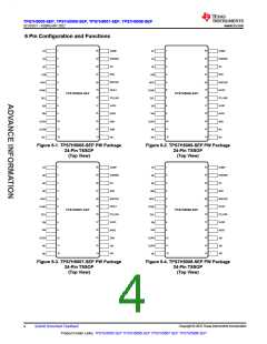
Table 6-1. Pin Functions
PIN
I/O
DESCRIPTION
TPS7H5005-
SEP
TPS7H5006-
SEP
TPS7H5007-
SEP
TPS7H5008-
SEP
In internal oscillation mode, the RT
pin must be populated with a resistor
to AVSS. When the RT pin is
floating, a 200-kHz to 4-MHz external
clock is required at the SYNC pin.
The frequency of the external clock
must be twice the desired switching
frequency.
RT
1
1
1
1
I/O
Primary off to synchronous rectifier on
dead-time set. Programmable through
an external resistor to AVSS.
PS
SP
2
3
4
2
3
4
—
—
—
—
—
4
I/O
I/O
I/O
Synchronous rectifier off to primary on
dead-time set. Programmable through
an external resistor to AVSS.
Leading edge blank time set.
Programmable through an external
resistor to AVSS.
LEB
Cycle-by-cycle current limit time delay
and hiccup time setting. Delay
time and hiccup time determined
by capacitor from HICC to AVSS.
Connecting this pin to AVSS disables
hiccup mode.
HICC
5
5
5
5
I/O
When the RT pin is floating, SYNC is
configured as an input for a 200-kHz
to 4-MHz external clock. In this case,
the external clock input gets inverted
and the system clock will run at half
the frequency of the external clock
input. When the RT pin is populated
with a resistor to AVSS, SYNC outputs
a 200-kHz to 4-MHz clock signal at
twice the device switching frequency
in phase with the switching of the
device.
SYNC
6
6
6
6
I/O
Duty cycle limit configurability. For
TPS7H5005-SEP, connect to AVSS for
50% duty cycle limit, floating for 75%,
and VLDO for 100%. For TPS7H5006-
SEP and TPS7H5007-SEP, the DCL
pin can be left floating or connected
to VLDO to set the maximum duty
cycle to 75% or 100%, respectively.
For TPS7H5008-SEP, this pin must be
connected to AVSS in order to obtain
the 50% maximum duty cycle.
DCL
7
7
7
7
I/O
Connecting the EN pin to the VLDO
pin or external source greater than 0.6
V enables the device. In addition, input
undervoltage lockout (UVLO) can be
adjusted with two resistors.
EN
8
8
8
8
I
Input supply to the device. Input
voltage range is from 4 V to 14 V.
VIN
9
9
9
9
I
OUTA
OUTB
10
11
10
—
10
—
10
11
O
O
Primary switching output A.
Primary switching output B. Active
only when DCL = AVSS.
Synchronous rectifier output B. Active
only when DCL = AVSS.
SRB
14
—
—
—
O
Copyright © 2022 Texas Instruments Incorporated
Submit Document Feedback
5
Product Folder Links: TPS7H5005-SEP TPS7H5006-SEP TPS7H5007-SEP TPS7H5008-SEP

 TI [ TEXAS INSTRUMENTS ]