TPS7A80xx
www.ti.com
SBVS135A –JUNE 2010–REVISED JUNE 2010
Undervoltage Lock-Out (UVLO)
Power dissipation of the device depends on input
voltage and load conditions and can be calculated
using Equation 4:
The TPS7A80xx utilizes an undervoltage lock-out
circuit to keep the output shut off until the internal
circuitry is operating properly. The UVLO circuit has a
de-glitch feature so that it typically ignores
undershoot transients on the input if they are less
than 50ms duration.
ǒ
Ǔ
PD + VIN * VOUT IOUT
(4)
Power dissipation can be minimized and greater
efficiency can be achieved by using the lowest
possible input voltage necessary to achieve the
required output voltage regulation.
Minimum Load
On the SON (DRB) package, the primary conduction
path for heat is through the exposed pad to the
printed circuit board (PCB). The pad can be
connected to ground or be left floating; however, it
should be attached to an appropriate amount of
copper PCB area to ensure the device does not
overheat. The maximum junction-to-ambient thermal
resistance depends on the maximum ambient
temperature, maximum device junction temperature,
and power dissipation of the device and can be
calculated using Equation 5:
The TPS7A80xx is stable and well-behaved with no
output load. Traditional PMOS LDO regulators suffer
from lower loop gain at very light output loads. The
TPS7A80xx employs an innovative low-current mode
circuit to increase loop gain under very light or
no-load conditions, resulting in improved output
voltage regulation performance down to zero output
current.
THERMAL INFORMATION
Thermal Protection
O
(
)
)125 C * TA
R
+
qJA
PD
(5)
Thermal protection disables the output when the
junction temperature rises to approximately +160°C,
allowing the device to cool. When the junction
temperature cools to approximately +140°C the
output circuitry is again enabled. Depending on power
dissipation, thermal resistance, and ambient
temperature, the thermal protection circuit may cycle
on and off. This cycling limits the dissipation of the
regulator, protecting it from damage because of
overheating.
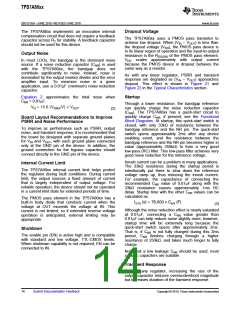
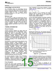
Knowing the maximum RqJA, the minimum amount of
PCB copper area needed for appropriate heatsinking
can be estimated using Figure 33.
160
140
120
100
80
Any tendency to activate the thermal protection circuit
indicates excessive power dissipation or an
inadequate heatsink. For reliable operation, junction
temperature should be limited to +125°C maximum.
To estimate the margin of safety in a complete design
60
40
20
(including
heatsink),
increase
the
ambient
temperature until the thermal protection is triggered;
use worst-case loads and signal conditions. For good
reliability, thermal protection should trigger at least
+35°C above the maximum expected ambient
condition of your particular application. This
0
0
1
2
3
4
5
6
7
8
9
10
Board Copper Area (in2)
Note: qJA value at board size of 9in2 (that is, 3in ×
3in) is a JEDEC standard.
configuration produces
a
worst-case junction
temperature of +125°C at the highest expected
ambient temperature and worst-case load.
Figure 33. qJA vs Board Size
The internal protection circuitry of the TPS7A80xx
has been designed to protect against overload
conditions. It was not intended to replace proper
heatsinking. Continuously running the TPS7A80xx
into thermal shutdown degrades device reliability.
Figure 33 shows the variation of qJA as a function of
ground plane Copper area in the board. It is intended
only as a guideline to demonstrate the effect of heat
spreading in the ground plane and should not be
used in a estimating the thermal performance in real
application environment.
Power Dissipation
NOTE: When the device is mounted on an
application PCB, it is strongly recommended to use
ΨJT and ΨJB, as explained in the Estimating Junction
Temperature section.
Knowing the device power dissipation and proper
sizing of the thermal plane that is connected to the
tab or pad is critical to avoiding thermal shutdown
and ensuring reliable operation.
Copyright © 2010, Texas Instruments Incorporated
Submit Documentation Feedback
15

 TI [ TEXAS INSTRUMENTS ]