TPS7A80xx
www.ti.com
SBVS135A –JUNE 2010–REVISED JUNE 2010
APPLICATION INFORMATION
The TPS7A80xx belongs to
a
family of new
For the adjustable version (TPS7A8001), the voltage
on the FB pin sets the output voltage and is
determined by the values of R1 and R2. The values of
R1 and R2 can be calculated for any voltage using the
formula given in Equation 1:
generation LDO regulators that use innovative
circuitry to achieve ultra-wide bandwidth and high
loop gain, resulting in extremely high PSRR (over a
1MHz range) at very low headroom (VIN – VOUT). A
noise reduction capacitor (CNR) at the NR pin
bypasses noise generated by the bandgap reference
in order to improve PSRR, while a quick-start circuit
fast-charges this capacitor. This family of regulators
offers sub-bandgap output voltages, current limit, and
thermal protection, and is fully specified from –40°C
to +125°C.
(R1 + R2 )
VOUT
=
x 0.800
R2
(1)
Sample resistor values for common output voltages
are shown in Table 2. In Table 2, E96 series resistors
are used, and all values meet 1% of the target VOUT
,
assuming resistors with zero error. For the actual
design, pay attention to any resistor error factors.
Using lower values for R1 and R2 reduces the noise
injected from the FB pin.
Figure 31 shows the basic circuit connections for the
fixed voltage options. Figure 32 gives the connections
for the adjustable output version (TPS7A8001).
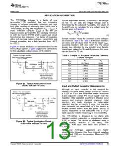
Optional 1.0mF input capacitor.
May improve source impedance,
noise, or PSRR.
Table 2. Sample 1% Resistor Values for Common
Output Voltages
VOUT
0.8V
1.0V
1.2V
1.5V
1.8V
2.5V
3.3V
5.0V
R1
R2
VIN
VOUT
IN
OUT
SNS
NR
0Ω (Short)
2.49kΩ
4.99kΩ
8.87kΩ
12.5kΩ
21.0kΩ
30.9kΩ
52.3kΩ
10.0kΩ
10.0kΩ
10.0kΩ
10.0kΩ
10.0kΩ
10.0kΩ
10.0kΩ
10.0kΩ
TPS7A80xx
4.7mF
Ceramic
EN
GND
VEN
To avoid inrush current,
it is recommended to
always connect a
1nF to 10nF capacitor
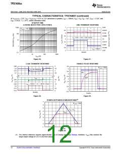
Figure 31. Typical Application Circuit
(Fixed Voltage Versions)
Input and Output Capacitor Requirements
Although an input capacitor is not required for
stability, it is good analog design practice to connect
a 0.1mF to 1.0mF low equivalent series resistance
(ESR) capacitor across the input supply near the
regulator. This capacitor counteracts reactive input
sources and improves transient response, noise
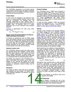
Optional 1.0mF input capacitor.
May improve source impedance,
noise, or PSRR.
VIN
VOUT
IN
OUT
R1
R2
4.7mF
Ceramic
TPS7A8001
rejection, and ripple rejection.
A
higher-value
EN
FB
capacitor may be necessary if large, fast rise-time
load transients are anticipated or if the device is
located several inches from the power source. If
source impedance is not sufficiently low, a 0.1mF
input capacitor may be necessary to ensure stability.
GND
NR
VEN
To avoid inrush current,
it is recommended to
always connect a
The TPS7A80xx is designed to be stable with
standard ceramic capacitors of capacitance values
4.7mF or larger. This device is evaluated using a
4.7mF ceramic capacitor of 10V rating, 10%
tolerance, X5R type, and 0805 size (2.0mm x
1.25mm).
1nF to 10nF capacitor
Figure 32. Typical Application Circuit
(Adjustable Voltage Version)
X5R- and X7R-type capacitors are highly
recommended because they have minimal variation
in value and ESR over temperature. Maximum ESR
should be <1.0Ω.
Copyright © 2010, Texas Instruments Incorporated
Submit Documentation Feedback
13

 TI [ TEXAS INSTRUMENTS ]