TPS7A80xx
SBVS135A –JUNE 2010–REVISED JUNE 2010
www.ti.com
The TPS7A80xx implements an innovative internal
compensation circuit that does not require a feedback
capacitor across R2 for stability. A feedback capacitor
should not be used for this device.
Dropout Voltage
The TPS7A80xx uses a PMOS pass transistor to
achieve low dropout. When (VIN – VOUT) is less than
the dropout voltage (VDO), the PMOS pass device is
in its linear region of operation and the input-to-output
resistance is the RDS(ON) of the PMOS pass element.
VDO scales approximately with output current
because the PMOS device in dropout behaves the
same way as a resistor.
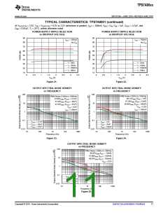
Output Noise
In most LDOs, the bandgap is the dominant noise
source. If a noise reduction capacitor (CNR) is used
with the TPS7A80xx, the bandgap does not
contribute significantly to noise. Instead, noise is
dominated by the output resistor divider and the error
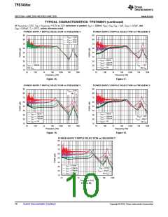
As with any linear regulator, PSRR and transient
response are degraded as (VIN – VOUT) approaches
dropout. This effect is shown in Figure 21 and
Figure 22 in the Typical Characteristics section.
amplifier input. To minimize noise in
a given
application, use a 0.01mF (minimum) noise-reduction
capacitor.
Equation
CNR = 0.01mF:
VN = 15.6 (VRMS/V) ´ VOUT
2
approximates the total noise when
Startup
Through a lower resistance, the bandgap reference
can quickly charge the noise reduction capacitor
(CNR). The TPS7A80xx has a quick-start circuit to
quickly charge CNR, if present; see the Functional
Block Diagrams. At startup, this quick-start switch is
closed, with only 33kΩ of resistance between the
bandgap reference and the NR pin. The quick-start
switch opens approximately 2ms after any device
enabling event, and the resistance between the
bandgap reference and the NR pin becomes higher in
value (approximately 250kΩ) to form a very good
low-pass (RC) filter. This low-pass filter achieves very
good noise reduction for the reference voltage.
(2)
Board Layout Recommendations to Improve
PSRR and Noise Performance
To improve ac performance such as PSRR, output
noise, and transient response, it is recommended that
the board be designed with separate ground planes
for VIN and VOUT, with each ground plane connected
only at the GND pin of the device. In addition, the
ground connection for the bypass capacitor should
connect directly to the GND pin of the device.
Inrush current can be a problem in many applications.
The 33kΩ resistance during the startup period is
intentionally put there to slow down the reference
voltage ramp up, thus reducing the inrush current.
For example, the capacitance of connecting the
recommended CNR value of 0.01mF along with the
33kΩ resistance causes approximately 1ms RC
delay. Startup time with the other CNR values can be
calculated as:
Internal Current Limit
The TPS7A80xx internal current limit helps protect
the regulator during fault conditions. During current
limit, the output sources a fixed amount of current
that is largely independent of output voltage. For
reliable operation, the device should not be operated
in a current limit state for extended periods of time.
The PMOS pass element in the TPS7A80xx has a
built-in body diode that conducts current when the
voltage at OUT exceeds the voltage at IN. This
current is not limited, so if extended reverse voltage
operation is anticipated, external limiting may be
appropriate.
tSTR (s) = 76,000 x CNR (F)
(3)
Although the noise reduction effect is nearly saturated
at 0.01mF, connecting a CNR value greater than
0.01mF can help reduce noise slightly more; however,
startup time will be extremely long because the
quick-start switch opens after approximately 2ms.
That is, if CNR is not fully charged during this 2ms
period, CNR finishes charging through a higher
resistance of 250kΩ, and takes much longer to fully
charge.
Shutdown
The enable pin (EN) is active high and is compatible
with standard and low voltage, TTL-CMOS levels.
When shutdown capability is not required, EN can be
connected to IN.
Note that a low leakage CNR should be used; most
ceramic capacitors are suitable.
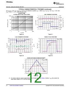
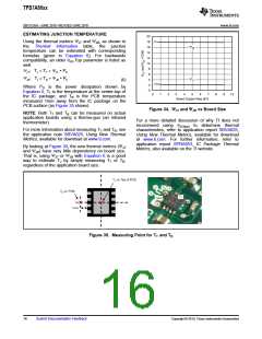
Transient Response
As with any regulator, increasing the size of the
output capacitor reduces over/undershoot magnitude
but increases duration of the transient response.
14
Submit Documentation Feedback
Copyright © 2010, Texas Instruments Incorporated

 TI [ TEXAS INSTRUMENTS ]