TPS7A80xx
SBVS135A –JUNE 2010–REVISED JUNE 2010
www.ti.com
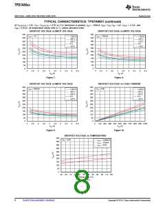
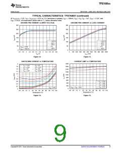
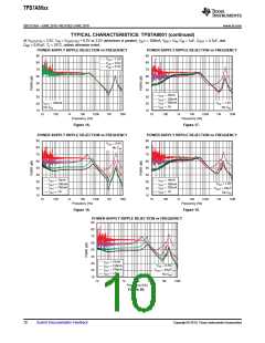
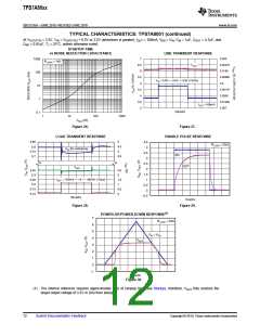
TYPICAL CHARACTERISTICS: TPS7A8001 (continued)
At VOUT(TYP) = 3.3V, VIN = VOUT(TYP) + 0.5V or 2.2V (whichever is greater), IOUT = 100mA, VEN = VIN, CIN = 1mF, COUT = 4.7mF, and
CNR = 0.01mF, TJ = 25°C, unless otherwise noted.
STARTUP TIME
vs NOISE REDUCTION CAPACITANCE
LINE TRANSIENT RESPONSE
7
6.5
6
3.333
1000
100
10
RLOAD = 1kW
3.32475
3.3165
3.30825
3.3
VOUT
5.5
5
VIN = 3.8V ® 4.8V ® 3.8V (1V/div)
4.5
4
3.29175
3.2835
3.27525
3.267
1
3.5
3
IOUT = 500mA
50ms/div
0.1
1
10
100
1000
CNR (nF)
Figure 26.
Figure 27.
LOAD TRANSIENT RESPONSE
ENABLE PULSE RESPONSE
3.85
5
4.5
4
RLOAD = 33W
3.8
3.75
3.7
4.5
4
VIN (for reference)
3.5
3
EN
3.5
2.5
2
OUT
VOUT
3.35
3.3
2.5
2
1.5
1
IOUT = 100mA ® 1A ® 100mA (1A/ms)
3.25
3.2
1.5
1
0.5
0
3.15
3.15
0.5
0
-0.5
50ms/div
1ms/div
Figure 28.
Figure 29.
POWER-UP/POWER-DOWN RESPONSE(1)
7
6
RLOAD = 33W
5
VIN = VEN
4
VOUT
3
2
1
0
-1
1ms/div
Figure 30.
(1) The internal reference requires approximately 2ms of rampup time (see Startup); therefore, VOUT fully reaches the
target output voltage of 3.3V in 2ms from starup.
12
Submit Documentation Feedback
Copyright © 2010, Texas Instruments Incorporated

 TI [ TEXAS INSTRUMENTS ]