TPS7A39
www.ti.com.cn
ZHCSGP0A –JULY 2017–REVISED SEPTEMBER 2017
For further details, see the How to Measure LDO Noise white paper.
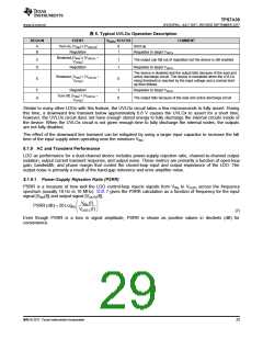
8.1.9.4 Optimizing Noise and PSRR
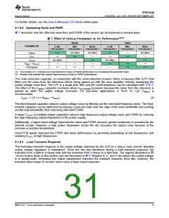
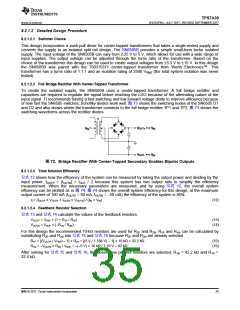
表 7 describes how the ultra-low noise floor and PSRR of the device can be improved in several ways.
表 7. Effect of Various Parameters on AC Performance(1)(2)
NOISE
PSRR
PARAMETER
LOW-
MID-
HIGH-
LOW-
MID-
HIGH-
FREQUENCY
FREQUENCY
FREQUENCY
FREQUENCY
FREQUENCY
FREQUENCY
CNR/SS
CFFx
+++
No effect
No effect
+++
++
+
No effect
+
++
No effect
+
+++
+
+
+++
+
+++
+
COUTx
No effect
+++
+++
++
|VINx| – |VOUTx
|
+
+++
+++
PCB layout
++
++
+
+
+++
(1) The number of +s indicates the improvement in noise or PSRR performance by increasing the parameter value.
(2) Shaded cells indicate the easiest improvement to noise or PSRR performance.
The noise-reduction capacitor, in conjunction with the noise-reduction resistor, forms a low-pass filter (LPF) that
filters out the noise from the reference before being gained up with the error amplifier, thereby minimizing the
output voltage noise floor. The LPF is a single-pole filter and the cutoff frequency can be calculated with 公式 8.
The effect of the CNR/SS capacitor increases when VOUTx(NOM) increases because the noise from the reference is
gained up when the output voltage increases. For low-noise applications, a 10-nF to 1-µF CNR/SS is
recommended.
fcutoff = 1 / (2 × π × RNR/SS × CNR/SS
)
(8)
The feed-forward capacitor reduces output voltage noise by filtering out the mid-band frequency noise. The feed-
forward capacitor can be optimized by placing a pole-zero pair near the edge of the loop bandwidth and pushing
out the loop bandwidth, thus improving mid-band PSRR.
A larger COUTx or multiple output capacitors reduces high-frequency output voltage noise and PSRR by reducing
the high-frequency output impedance of the power supply.
Additionally, a higher input voltage improves the noise and PSRR because greater headroom is provided for the
internal circuits. However, a high power dissipation across the die increases the output noise because of the
increase in junction temperature.
Good PCB layout improves the PSRR and noise performance by providing heatsinking at low frequencies and
isolating VOUTx at high frequencies.
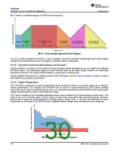
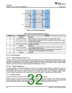
8.1.9.5 Load Transient Response
The load-step transient response is the output voltage response by the LDO to a step in load current, whereby
output voltage regulation is maintained. There are two key transitions during a load transient response: the
transition from a light to a heavy load and the transition from a heavy to a light load. The regions illustrated in 图
69 are broken down in this section and are described in 表 8. Regions A, E, and H are where the output voltage
is in steady-state. Increasing the output capacitance improves the transient response (less dip); however, the
transient takes longer to recover when using a large output capacitor.
版权 © 2017, Texas Instruments Incorporated
31

 TI [ TEXAS INSTRUMENTS ]